- 您現(xiàn)在的位置:買賣IC網(wǎng) > PDF目錄383086 > ICL7139 (Intersil Corporation) Quad LVDS Receiver with -2 to 4.4V Common-mode Range 16-SOIC -40 to 85 PDF資料下載
參數(shù)資料
| 型號: | ICL7139 |
| 廠商: | Intersil Corporation |
| 英文描述: | Quad LVDS Receiver with -2 to 4.4V Common-mode Range 16-SOIC -40 to 85 |
| 中文描述: | 33 / 4位,自動量程萬用表 |
| 文件頁數(shù): | 10/13頁 |
| 文件大?。?/td> | 111K |
| 代理商: | ICL7139 |
3-42
OSC OUT pin is not designed to drive large external loads,
loading on this pin should not exceed a single CMOS input.
The oscillator frequency is internally divided by two to gener-
ate the ICL7139 and ICL7149 clock. The frequency should
be 120kHz to reject 60Hz AC signals, and 100kHz to reject
50Hz signals.
Display Drivers
Figure 12 shows typical LCD Drive waveforms, RMS ON, and
RMS OFF voltage calculations. Duplex multiplexing is used to
minimize the number of connections between the ICL7139
and ICL7149 and the LCD. The LCD has two separate back-
planes. Each drive line can drive two individual segments, one
referenced to each backplane. The ICL7139 and ICL7149
drive 3
3
/
4
7-segment digits, 3 decimal points, and 11 annunci-
ators. Annunciators are used to indicate polarity, low battery
condition, and the range in use. Peak drive voltage across the
display is approximately 3V. An LCD with approximately
1.4V
RMS
threshold voltage should be used. The third voltage
level needed for duplex drive waveforms is generated through
an on-chip resistor string. The DC component of the drive
waveforms is guaranteed to be less than 50mV.
Ternary Input
The
/Volts/Amps logic input is a ternary, or 3-level input.
This input is internally tied to the common voltage through a
high-value resistor, and will go to the middle, or “Volts” state,
when not externally connected. When connected to V-,
approximately 5
μ
A of current flows out of the input. In this
case, the logic level is the “Amps”, or low state. When con-
nected to V+, about 5
μ
A of current flows into the input. Here,
the logic level is the “
”, or high state. For other pins, see
Table 2.
Component Selection
For optimum performance while maintaining the low-cost
advantages of the ICL7139 and ICL7149, care must be
taken when selecting external components. This section
reviews specifications and performance effects of various
external components.
5M
330K
10pF
5pF
OSC OUT
OSC IN
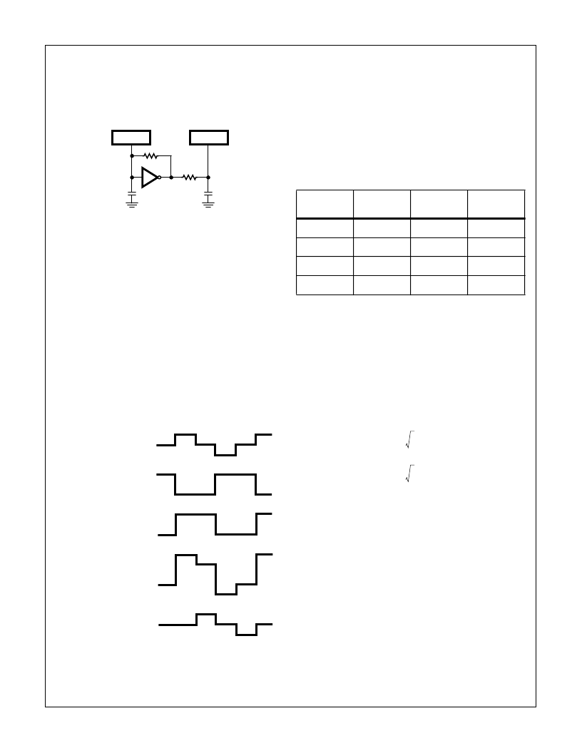
FIGURE 11. INTERNAL OSCILLATOR CIRCUIT DIAGRAM
TABLE 2. TERNARY INPUTS CONNECTIONS
PIN
NUMBER
V+
OPEN
OR COM
V-
17
mA
μ
A
Test
18
V
Amps
19
Hi
/DC
Lo
/AC
Test
20
Hold
Auto
Test
BACKPLANE
SEGMENT ON
SEGMENT OFF
V
SEGMENT ON
V
SEGMENT OFF
V
PEAK
V
PEAK/2
O
V
PEAK
O
V
PEAK
O
2V
PEAK
O
(VOLTAGE ACROSS ON SEGMENT)
(VOLTAGE ACROSS OFF SEGMENT)
-2V
PEAK
V
PEAK
O
-V
PEAK
V+
DCOM
V
PEAK
= 3V
±
10%
RMS ON
→
2.37V
RMS OFF
→
1.06V
V
RMS
5
8
--
V
PEAK
ON
=
V
RMS
5
8
--
V
PEAK
OFF
=
FIGURE 12. DUPLEXED LCD DRIVE WAVEFORMS
ICL7139, ICL7149
相關(guān)PDF資料 |
PDF描述 |
|---|---|
| ICL7139CPL | Quad LVDS Receiver with -2 to 4.4V Common-mode Range 16-SOIC -40 to 85 |
| ICL7149 | Quad LVDS Receiver with -4 to 5V Common-mode Range 24-TSSOP -40 to 85 |
| ICL7149CPL | 33/4 Digit, Autoranging Multimeter |
| ICL7611DCPA | 1.4MHz, Low Power CMOS Operational Amplifiers |
| ICL7611ACJD | Single/Dual/Triple/Quad Operational Amplifiers |
相關(guān)代理商/技術(shù)參數(shù) |
參數(shù)描述 |
|---|---|
| ICL7139CM44 | 制造商:Rochester Electronics LLC 功能描述:- Bulk 制造商:Harris Corporation 功能描述: |
| ICL7139CPL | 制造商:Harris Corporation 功能描述: |
| ICL7139CPL WAF | 制造商:Harris Corporation 功能描述: |
| ICL7139IM44 | 制造商:未知廠家 制造商全稱:未知廠家 功能描述:Converter IC |
| ICL7139IPL | 制造商:未知廠家 制造商全稱:未知廠家 功能描述:Converter IC |
發(fā)布緊急采購,3分鐘左右您將得到回復(fù)。