- 您現(xiàn)在的位置:買賣IC網(wǎng) > PDF目錄383083 > ICL3310CB (INTERSIL CORP) +3V to +5.5V, 1 Microamp, 250kbps, RS-232 Transmitter/Receiver PDF資料下載
參數(shù)資料
| 型號(hào): | ICL3310CB |
| 廠商: | INTERSIL CORP |
| 元件分類: | 通用總線功能 |
| 英文描述: | +3V to +5.5V, 1 Microamp, 250kbps, RS-232 Transmitter/Receiver |
| 中文描述: | DUAL LINE TRANSCEIVER, PDSO18 |
| 封裝: | PLASTIC, SOIC-18 |
| 文件頁數(shù): | 4/9頁 |
| 文件大小: | 158K |
| 代理商: | ICL3310CB |
4
Detailed Description
ICL3310 interface ICs operate from a single +3V to +5.5V
supply, guarantee a 250kbps minimum data rate, require
only four small external 0.1
μ
F capacitors, feature low power
consumption, and meet all ElA RS-232C and V.28
specifications. The circuit is divided into three sections: The
charge pump, the transmitters, and the receivers.
Charge-Pump
Intersil’s new ICL3310 utilizes regulated on-chip dual charge
pumps as voltage doublers, and voltage inverters to
generate
±
5.5V transmitter supplies from a V
CC
supply as
low as 3.0V. This allows these devices to maintain RS-232
compliant output levels over the
±
10% tolerance range of
3.3V powered systems. The efficient on-chip power supplies
require only four small, external 0.1
μ
F capacitors for the
voltage doubler and inverter functions at V
CC
= 3.3V. See
the “Capacitor Selection” section, and Table 3 for capacitor
recommendations for other operating conditions. The charge
pumps operate discontinuously (i.e., they turn off as soon as
the V+ and V- supplies are pumped up to the nominal
values), resulting in significant power savings.
Transmitters
The transmitters are proprietary, low dropout, inverting
drivers that translate TTL/CMOS inputs to EIA/TIA-232
output levels. Coupled with the on-chip
±
5.5V supplies,
these transmitters deliver true RS-232 levels over a wide
range of single supply system voltages.
All transmitter outputs disable and assume a high
impedance state when the device enters the powerdown
mode (see Table 2). These outputs may be driven to
±
12V
when disabled.
All devices guarantee a 250kbps data rate for full load
conditions (3k
and 1000pF), V
CC
≥
3.0V, with one
transmitter operating at full speed. Under more typical
conditions of V
CC
≥
3.3V, R
L
= 3k
, and C
L
= 250pF, one
transmitter easily operates at 900kbps.
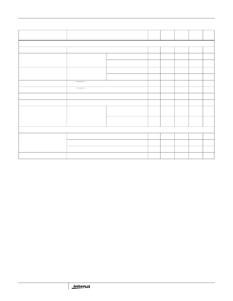
TIMING CHARACTERISTICS
Maximum Data Rate
R
L
= 3k
,
C
L
= 1000pF, One Transmitter Switching
Full
250
500
-
kbps
Transmitter Propagation Delay
Transmitter Input to
Transmitter Output,
C
L
= 1000pF
t
PHL
Full
-
0.6
3.5
μ
s
t
PLH
Full
-
0.7
3.5
μ
s
Receiver Propagation Delay
Receiver Input to Receiver
Output, C
L
= 150pF
t
PHL
Full
-
0.2
1
μ
s
t
PLH
Full
-
0.3
1
μ
s
Transmitter Output Enable Time
From SHDN Rising Edge to T
OUT
=
±
3V
25
-
50
-
μ
s
Transmitter Output Disable Time
From SHDN Falling Edge to T
OUT
=
±
5V
25
-
600
-
ns
Transmitter Skew
t
PHL
- t
PLH
(Note 2)
25
-
100
-
ns
Receiver Skew
t
PHL
- t
PLH
25
-
100
-
ns
Transition Region Slew Rate
R
L
= 3k
to 7k
,
Measured From 3V to -3V
or -3V to 3V
V
CC
= 3.3V,
C
L
= 150pF to 2500pF
25
4
-
-
V/
μ
s
V
CC
= 4.5V,
C
L
= 150pF to 2500pF
25
6
-
-
V/
μ
s
ESD PERFORMANCE
RS-232 Pins (T
OUT
, R
IN
)
Human Body Model
25
-
±
15
-
kV
IEC1000-4-2 Contact Discharge
25
-
±
8
-
kV
IEC1000-4-2 Air Gap Discharge
25
-
>±
8
-
kV
All Other Pins
Human Body Model
25
-
±
3
-
kV
NOTE:
2. Transmitter skew is measured at the transmitter zero crossing points.
Electrical Specifications
Test Conditions: V
= 3V to 5.5V, C
- C
4
= 0.1
μ
F; Unless Otherwise Specified.
Typicals are at T
A
= 25
C
(Continued)
PARAMETER
TEST CONDITIONS
TEMP
(
o
C)
MIN
TYP
MAX
UNITS
ICL3310
相關(guān)PDF資料 |
PDF描述 |
|---|---|
| ICL3310CB-T | +3V to +5.5V, 1 Microamp, 250kbps, RS-232 Transmitter/Receiver |
| ICL3310IB | +3V to +5.5V, 1 Microamp, 250kbps, RS-232 Transmitter/Receiver |
| ICL3310IB-T | +3V to +5.5V, 1 Microamp, 250kbps, RS-232 Transmitter/Receiver |
| ICL7104-14 | 14-BitMicroprocessor-Compatible, 2-Chip, A/D Converter(14位、微處理器兼容的2片A/D轉(zhuǎn)換器) |
| ICL8052 | 14-Bit/16-Bit, Microprocessor- Compatible, 2-Chip, A/D Converter |
相關(guān)代理商/技術(shù)參數(shù) |
參數(shù)描述 |
|---|---|
| ICL3310CB-T | 制造商:INTERSIL 制造商全稱:Intersil Corporation 功能描述:+3V to +5.5V, 1 Microamp, 250kbps, RS-232 Transmitter/Receiver |
| ICL3310E | 制造商:INTERSIL 制造商全稱:Intersil Corporation 功能描述:+/- 15kV ESD Protected, +3V to +5.5V, 1 Microamp, 250kbps, RS-232 Transmitter/Receiver |
| ICL3310ECA | 制造商:INTERSIL 制造商全稱:Intersil Corporation 功能描述:+/- 15kV ESD Protected, +3V to +5.5V, 1 Microamp, 250kbps, RS-232 Transmitter/Receiver |
| ICL3310ECA-T | 制造商:INTERSIL 制造商全稱:Intersil Corporation 功能描述:+/- 15kV ESD Protected, +3V to +5.5V, 1 Microamp, 250kbps, RS-232 Transmitter/Receiver |
| ICL3310ECB | 制造商:Rochester Electronics LLC 功能描述:RS232 3V 2D/2R 15KV SHUTDOWN 18SOIC COM - Bulk 制造商:Intersil Corporation 功能描述: |
發(fā)布緊急采購,3分鐘左右您將得到回復(fù)。