- 您現(xiàn)在的位置:買賣IC網(wǎng) > PDF目錄360703 > IBM25PPC750L-GB333C2ST Microprocessor PDF資料下載
參數(shù)資料
| 型號: | IBM25PPC750L-GB333C2ST |
| 英文描述: | Microprocessor |
| 中文描述: | 微處理器 |
| 文件頁數(shù): | 34/50頁 |
| 文件大小: | 516K |
| 代理商: | IBM25PPC750L-GB333C2ST |
第1頁第2頁第3頁第4頁第5頁第6頁第7頁第8頁第9頁第10頁第11頁第12頁第13頁第14頁第15頁第16頁第17頁第18頁第19頁第20頁第21頁第22頁第23頁第24頁第25頁第26頁第27頁第28頁第29頁第30頁第31頁第32頁第33頁當前第34頁第35頁第36頁第37頁第38頁第39頁第40頁第41頁第42頁第43頁第44頁第45頁第46頁第47頁第48頁第49頁第50頁
Page 30
Version 1.51
PowerPC 740 and PowerPC 750 Datasheet
5/20/99
PowerPC 740 and PowerPC 750 Embedded Microprocessor
IBM CMOS 0.20 um Copper Technology EMPPC740L and EMPPC750L
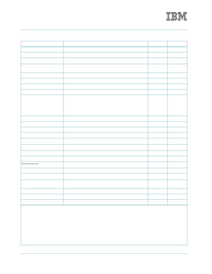
HRESET
B6
Low
Input
INT
C11
Low
Input
L1_TSTCLK
1
F8
High
Input
L2ADDR[0-16]
L17, L18, L19, M19, K18, K17, K15, J19, J18, J17, J16, H18, H17,
J14, J13, H19, G18
High
Output
L2AVDD
L13
—
—
L2CE
P17
Low
Output
L2CLKOUTA
N15
—
Output
L2CLKOUTB
L16
—
Output
L2DATA[0-63]
U14, R13, W14, W15, V15, U15, W16, V16, W17, V17, U17, W18,
V18, U18, V19, U19, T18, T17, R19, R18, R17, R15, P19, P18, P13,
N14, N13, N19, N17, M17, M13, M18, H13, G19, G16, G15, G14,
G13, F19, F18, F13, E19, E18, E17, E15, D19, D18, D17, C18, C17,
B19, B18, B17, A18, A17, A16, B16, C16, A14, A15, C15, B14, C14,
E13
High
I/O
L2DP[0-7]
V14, U16, T19, N18, H14, F17, C19, B15
High
I/O
L2OVDD
D15, E14, E16, H16, J15, L15, M16, P15, R14, R16, T15, F15
—
—
L2SYNC_IN
L14
—
Input
L2SYNC_OUT
M14
—
Output
L2_TSTCLK
1,5
F7
High
Input
L2VSEL
A19
6
—
Input
L2WE
N16
Low
Output
L2ZZ
G17
High
Output
LSSD_MODE
1
F9
Low
Input
MCP
B11
Low
Input
NC (No-Connect)
B3, B4, B5, W19, K9, K11
4
, K19
4
—
—
OVDD
2
D5, D8, D12, E4, E6, E9, E11, F5, H4, J5, L5, M4, P5, R4, R6, R9,
R11, T5, T8, T12
—
—
PLL_CFG[0-3]
A4, A5, A6, A7
High
Input
QACK
B2
Low
Input
QREQ
J3
Low
Output
Pinout Listing for the 360 CBGA package (cont.)
Signal Name
Pin Number
Active
I/O
Note:
1. These are test signals for factory use only and must be pulled up to OV
DD
for normal machine operation.
2. OV
DD
inputs supply power to the I/O drivers and V
DD
inputs supply power to the processor core.
3. Internally tied to L2OV
DD
in the 750 360 CBGA package. This is NOT a supply pin.
4. These pins are reserved for potential future use as additional L2 address pins.
5. L2_TSTCLK may be tied to ground for normal machine operation, if extra 60x bus output hold is required on all 60x bus signals. See Table “60X Bus
Output AC Timing Specifications for the 750
,” on page 14, spec 15.
6. These pins are no connects on dd2.x and have no function. They will be added to dd3.x to select voltage levels for the L2 bus (A19) and the rest of the
I/O (W01). Leaving the pin unconnected will select the normal supply value. Connecting these pins to HRESET# or ground on dd3.x will select lower
voltage supply ranges.
Powered by ICminer.com Electronic-Library Service CopyRight 2003
相關(guān)PDF資料 |
PDF描述 |
|---|---|
| IBM25PPC750L-GB333C2T | Microprocessor |
| IBM25PPC750L-GB333D2R | Microprocessor |
| IBM25PPC750L-GB333D2SR | Microprocessor |
| IBM25PPC750L-GB333D2ST | Microprocessor |
| IBM25PPC750L-GB333D2T | Microprocessor |
相關(guān)代理商/技術(shù)參數(shù) |
參數(shù)描述 |
|---|---|
| IBM25PPC750L-GB333C2T | 制造商:未知廠家 制造商全稱:未知廠家 功能描述:Microprocessor |
| IBM25PPC750L-GB333D2R | 制造商:未知廠家 制造商全稱:未知廠家 功能描述:Microprocessor |
| IBM25PPC750L-GB333D2SR | 制造商:未知廠家 制造商全稱:未知廠家 功能描述:Microprocessor |
| IBM25PPC750L-GB333D2ST | 制造商:未知廠家 制造商全稱:未知廠家 功能描述:Microprocessor |
| IBM25PPC750L-GB333D2T | 制造商:未知廠家 制造商全稱:未知廠家 功能描述:Microprocessor |
發(fā)布緊急采購,3分鐘左右您將得到回復(fù)。