- 您現(xiàn)在的位置:買賣IC網(wǎng) > PDF目錄67683 > IBM25PPC750CXEJP7012T 32-BIT, 600 MHz, RISC PROCESSOR, PBGA256 PDF資料下載
參數(shù)資料
| 型號(hào): | IBM25PPC750CXEJP7012T |
| 元件分類: | 微控制器/微處理器 |
| 英文描述: | 32-BIT, 600 MHz, RISC PROCESSOR, PBGA256 |
| 封裝: | 27 X 27 MM, PLASTIC, BGA-256 |
| 文件頁數(shù): | 29/44頁 |
| 文件大?。?/td> | 416K |
| 代理商: | IBM25PPC750CXEJP7012T |
第1頁第2頁第3頁第4頁第5頁第6頁第7頁第8頁第9頁第10頁第11頁第12頁第13頁第14頁第15頁第16頁第17頁第18頁第19頁第20頁第21頁第22頁第23頁第24頁第25頁第26頁第27頁第28頁當(dāng)前第29頁第30頁第31頁第32頁第33頁第34頁第35頁第36頁第37頁第38頁第39頁第40頁第41頁第42頁第43頁第44頁
Data Sheet
Preliminary
PowerPC 750CXe RISC Microprocessor
750cxe_DD3.1_Dev_3_gen_mkt.fm.1.5
April 8, 2004
System Design Information
Page 27 of 36
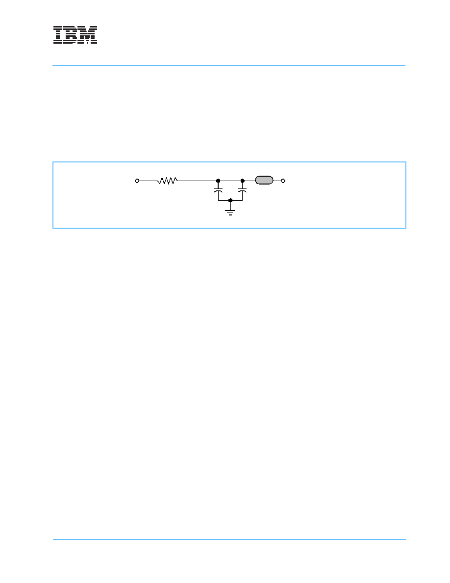
6.2 PLL Power Supply Filtering
The AVDD power signal is provided on the PowerPC 750CXe to provide power to the clock generation phase-
locked loop. To ensure stability of the internal clock, the power supplied to the AVDD input signal should be
filtered using a circuit similar to the one shown in Figure 6-1. The circuit should be placed as close as
possible to the AVDD pin to ensure it filters out as much noise as possible. The referenced ferrite bead, FB,
shown in Figure 6-1 should supply an impedance of approximately 30
in the 100MHz region (Murata
BLM21P300S or similar).
6.3 Decoupling Recommendations
Due to the PowerPC 750CXe’s feature large address and data buses, and high operating frequencies, the
PowerPC 750CXe can generate transient power surges and high frequency noise in its power supply,
especially while driving large capacitive loads. This noise must be prevented from reaching other components
in the PowerPC 750CXe system, and the PowerPC 750CXe itself requires a clean, tightly regulated source of
power.
Therefore, it is strongly recommended that the system designer place at least one decoupling capacitor with
a low ESR (effective series resistance) rating at each VDD and OVDD pin of the PowerPC 750CXe. It is also
recommended that these decoupling capacitors receive their power from separate VDD, OVDD, and GND
power planes in the PCB, utilizing short traces to minimize inductance.
These capacitors should range in value from 220pF to 10
F to provide both high and low-frequency filtering,
and should be placed as close as possible to their associated VDD or OVDD pins. Suggested values for the
VDD pins: 220pF (ceramic X7R), 0.01
F (ceramic X7R), and 0.1f (ceramic X7R). Suggested values for the
OVDD pins: 0.01
F (ceramic X7R), 0.1f (ceramic X7R), and 10F (tantalum). Only SMT (surface-mount
technology) capacitors should be used to minimize lead inductance.
In addition, it is recommended that there be several bulk storage capacitors distributed around the PCB,
feeding the VDD and OVDD planes, to enable quick recharging of the smaller chip capacitors. These bulk
capacitors should have a low ESR (equivalent series resistance) rating to ensure the quick response time
necessary. They should also be connected to the power and ground planes through two vias to minimize
inductance.
Suggested bulk capacitors: 100
F (AVX TPS tantalum) or 330F (AVX TPS tantalum).
Figure 6-1. PLL Power Supply Filter Circuit
V
DD
AV
DD
2
10
F
0.1
F
GND
FB
相關(guān)PDF資料 |
PDF描述 |
|---|---|
| IBM25PPC750CXEJP5523T | 32-BIT, 533 MHz, RISC PROCESSOR, PBGA256 |
| IBM25PPC750CXEJQ5012T | 32-BIT, 500 MHz, RISC PROCESSOR, PBGA256 |
| IBM25PPC750CXEJQ4012T | 32-BIT, 466 MHz, RISC PROCESSOR, PBGA256 |
| IBM25PPC750CXEJQ2013T | 32-BIT, 400 MHz, RISC PROCESSOR, PBGA256 |
| IBM25PPC750CXEJP5513T | 32-BIT, 533 MHz, RISC PROCESSOR, PBGA256 |
相關(guān)代理商/技術(shù)參數(shù) |
參數(shù)描述 |
|---|---|
| IBM25PPC750CXEJP7013T | 制造商:IBM 功能描述:IBMIBM25PPC750CXEJP7013T OEM EOL151207 |
| IBM25PPC750FL-GR0123V | 制造商:IBM 功能描述:MPU 750XX RISC 32BIT - Trays |
| IBM25PPC750FL-GR0124V | 制造商:IBM 功能描述:MPU 750XX RISC 32BIT - Trays |
| IBM25PPC750FL-GR0133T | 制造商:IBM 功能描述:IBMIBM25PPC750FL-GR0133T CSOI9SG LOGIC P |
| IBM25PPC750FL-GR0133V | 制造商:IBM 功能描述:MPU 750XX RISC 32BIT - Trays |
發(fā)布緊急采購,3分鐘左右您將得到回復(fù)。