- 您現(xiàn)在的位置:買賣IC網(wǎng) > PDF目錄67682 > IBM25PPC740L-GB400A2T 32-BIT, 400 MHz, RISC PROCESSOR, CBGA255 PDF資料下載
參數(shù)資料
| 型號: | IBM25PPC740L-GB400A2T |
| 元件分類: | 微控制器/微處理器 |
| 英文描述: | 32-BIT, 400 MHz, RISC PROCESSOR, CBGA255 |
| 封裝: | 21 X 21 MM, 1.27 MM PITCH, CERAMIC, BGA-255 |
| 文件頁數(shù): | 5/48頁 |
| 文件大小: | 608K |
| 代理商: | IBM25PPC740L-GB400A2T |
第1頁第2頁第3頁第4頁當(dāng)前第5頁第6頁第7頁第8頁第9頁第10頁第11頁第12頁第13頁第14頁第15頁第16頁第17頁第18頁第19頁第20頁第21頁第22頁第23頁第24頁第25頁第26頁第27頁第28頁第29頁第30頁第31頁第32頁第33頁第34頁第35頁第36頁第37頁第38頁第39頁第40頁第41頁第42頁第43頁第44頁第45頁第46頁第47頁第48頁
12/8/99
Version 1.02
Page 13
PowerPC 740 and PowerPC 750 Microprocessor
CMOS 0.20
m Copper Technology, PID-8p, PPC740L and PPC750L, dd3.2
AC Electrical Characteristics
This section provides the AC electrical characteristics for the 750. After fabrication, parts are sorted by maxi-
mum processor core frequency as shown in the Section “Clock AC Specifications,” on page 13, and tested for
conformance to the AC specifications for that frequency. Parts are sold by maximum processor core fre-
quency, subject to the specified application conditions; see Section “Ordering Information,” on page 46.
Unless otherwise noted, all timings apply for all I/O supply voltages.
Clock AC Specications
The following table provides the clock AC timing specifications as defined in Figure 2.
Clock AC Timing Specications
See Table “Recommended Operating Conditions,” on page 9, for operating conditions.
Num
Characteristic
Fmax = 300-375MHz
Fmax
≥ 400MHz
Unit
Notes
Min
Max
Min
Max
Processor frequency
TBD
As specified by
part number
250
As specified by
part number
MHz
6
SYSCLK frequency
25
100
31
100
MHz
1
SYSCLK cycle time
10
40
10
32
ns
2,3
SYSCLK rise and fall time
–
1.0
–
1.0
ns
2,3
4
SYSCLK duty cycle measured
at Vm
40
60
40
60
%
3
SYSCLK jitter
–
±150
–
±150
ps
4,3
Internal PLL relock time
–
100
–
100
s5
Note:
1. Caution: The SYSCLK frequency and the PLL_CFG[0:3] settings must be chosen such that the resulting SYSCLK (bus) frequency, and CPU (core)
frequency do not exceed their respective maximum or minimum operating frequencies. Refer to the PLL_CFG[0:3] signal description in Section “PLL
Configuration,” on page 36 for valid PLL_CFG[0:3] settings. Bus operation above 100 MHz is possible, but requires careful timing analysis. Contact
IBM for details.
2. Rise and fall times for the SYSCLK input are measured from 0.5 to 1.5V.
3. Timing is guaranteed by design and characterization, and is not tested.
4. The total input jitter (short term and long term combined) must be under
±150ps. Contact IBM for operation with Spread Spectrum clocks or clocks
with more than
± 150 ps total jitter.
5. Relock timing is guaranteed by design and characterization, and is not tested. PLL-relock time is the maximum amount of time required for PLL lock
after a stable VDD and SYSCLK are reached during the power-on reset sequence. This specification also applies when the PLL has been disabled and
subsequently re-enabled during sleep mode. Also note that HRESET must be held asserted for a minimum of 255 bus clocks after the PLL-relock time
during the power-on reset sequence.
6. Under certain conditions, operation at core frequencies below those stated is possible. Contact IBM for details.
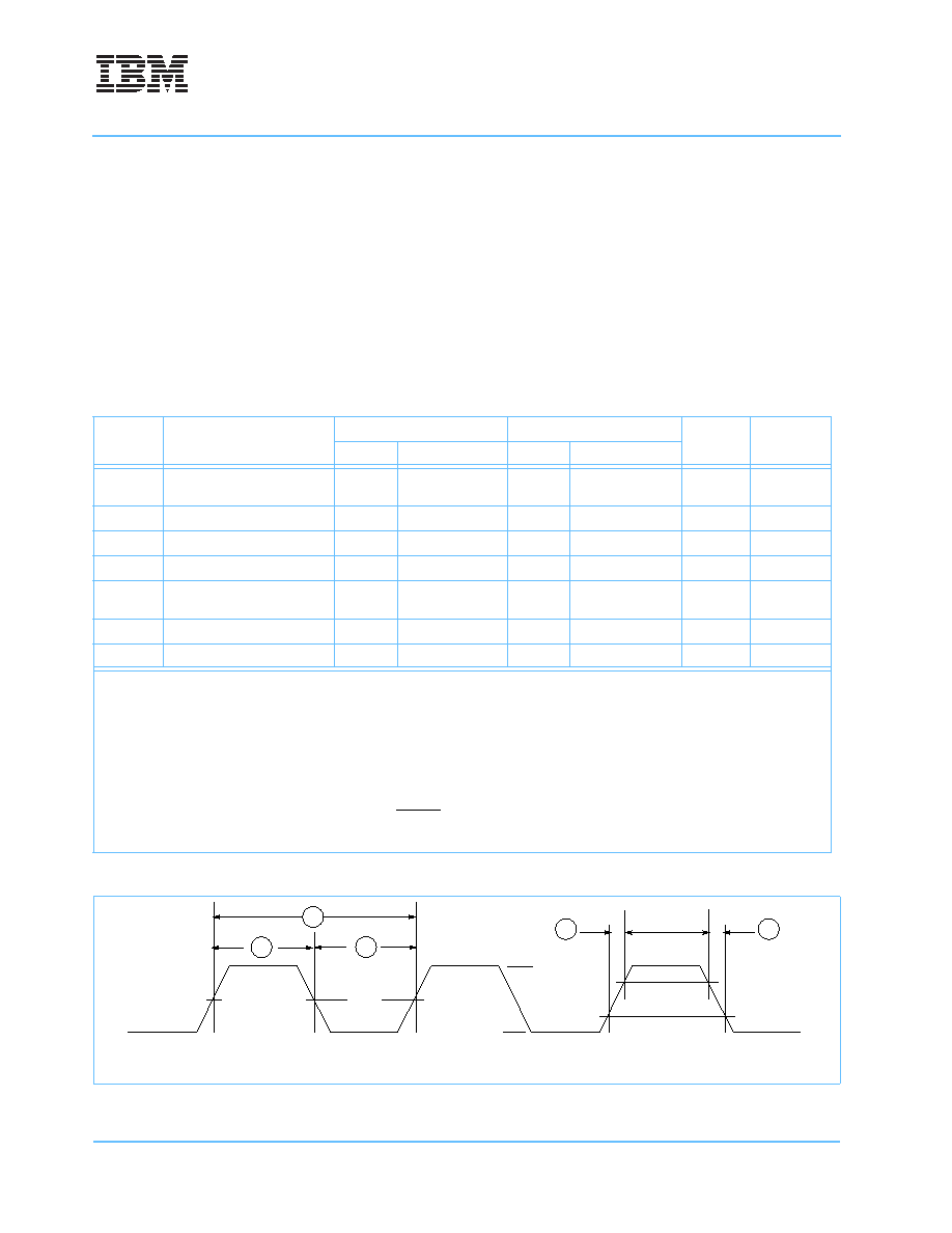
Figure 2. SYSCLK Input Timing Diagram
VM
CV
IL
CV
IH
1
2
4
3
4
SYSCLK
Vm = OVdd/2
相關(guān)PDF資料 |
PDF描述 |
|---|---|
| IBM25PPC750L-GB433A2R | 32-BIT, 433 MHz, RISC PROCESSOR, CBGA360 |
| IBM25PPC750L-GB350A2R | 32-BIT, 350 MHz, RISC PROCESSOR, CBGA360 |
| IBM25PPC750L-GB366A2R | 32-BIT, 366 MHz, RISC PROCESSOR, CBGA360 |
| IBM25PPC750L-GB375A2R | 32-BIT, 375 MHz, RISC PROCESSOR, CBGA360 |
| IBM25PPC750L-GB375A2T | 32-BIT, 375 MHz, RISC PROCESSOR, CBGA360 |
相關(guān)代理商/技術(shù)參數(shù) |
參數(shù)描述 |
|---|---|
| IBM25PPC740L-GB433A2R | 制造商:未知廠家 制造商全稱:未知廠家 功能描述:MICROPROCESSOR|32-BIT|CMOS|BGA|255PIN|CERAMIC |
| IBM25PPC740LGB433A2T | 制造商:IBM Microelectronics 功能描述:MPU PWRPC740 RISC 64BIT 0.2UM 433MHZ 1.8V/2.5V/3.3V 255CBGA - Trays 制造商:IBM 功能描述:IBM IBM25PPC740LGB433A2T Co-Processors |
| IBM25PPC740L-GB433A2T | 制造商:未知廠家 制造商全稱:未知廠家 功能描述:MICROPROCESSOR|32-BIT|CMOS|BGA|255PIN|CERAMIC |
| IBM25PPC740L-GB466A2R | 制造商:未知廠家 制造商全稱:未知廠家 功能描述:MICROPROCESSOR|32-BIT|CMOS|BGA|255PIN|CERAMIC |
| IBM25PPC740L-GB466A2T | 制造商:未知廠家 制造商全稱:未知廠家 功能描述:MICROPROCESSOR|32-BIT|CMOS|BGA|255PIN|CERAMIC |
發(fā)布緊急采購,3分鐘左右您將得到回復(fù)。