- 您現(xiàn)在的位置:買賣IC網(wǎng) > PDF目錄379201 > IAA110 (Clare, Inc.) Integrated Telecom Circuits PDF資料下載
參數(shù)資料
| 型號: | IAA110 |
| 廠商: | Clare, Inc. |
| 英文描述: | Integrated Telecom Circuits |
| 中文描述: | 綜合電信電路 |
| 文件頁數(shù): | 1/6頁 |
| 文件大小: | 402K |
| 代理商: | IAA110 |
1
www.clare.com
IAA110P
DS-IAA110P-R2
The IAA110P Multifunction Telecom switch combines two
350V Form Arelays and one optocoupler in a single pack-
age. The relay uses optically coupled MOSFET technolo-
gy to provide 1500V of input to output isolation. The
efficient MOSFET switches and photovoltaic die use
Clare’s patented OptoMOS architecture. The optically
coupled input uses highly efficient GaAIAs infrared LEDs.
IAA110P allows telecom circuit designers to combine
three discrete functions in a single component. The
IAA110P’s small package uses less space than tradition-
al discrete component solutions.
Telecommunications
Telecom Switching
Tip/Ring Circuits
Modem Switching (Laptop, Notebook, Pocket Size)
Hookswitch
Dial Pulsing
Ground Start
Ringer Injection
Instrumentation
Multiplexers
Data Acquisition
Electronic Switching
I/O Subsystems
Meters (Watt-Hour, Water, Gas)
Medical Equipment-Patient/Equipment Isolation
Security
Aerospace
Industrial Controls
UL Recognized: File Number E76270
CSA Certified: File Number LR 43639-12
VDE Compatible
BSI Certified:
BS EN 60950:1992 (BS7002:1992)
Certificate #:7969
BS EN 41003:1993
Certificate #:7969
Three Functions in One Package
Small 16 Pin SOIC Package (PCMCIA Compatible)
Bi-Directional Current Sensing
Bi-Directional Current Switching
3750V
RMS
Input/Output Isolation
FCC Compatible
No EMI/RFI Generation
Machine Insertable, Wave Solderable
Tape & Reel Versions Available
Applications
Features
Description
Approvals
Integrated Telecom Circuits
Ordering Information
Part #
IAA110P
IAA110PTR
Description
16 Pin SOIC (50/Tube)
16 Pin SOIC (1000/Reel)
IAA110P
350
100
35
Units
V
mA
Load Voltage
Load Current
Max R
ON
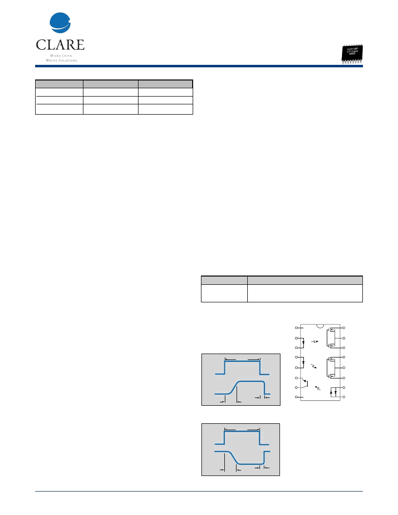
Pin Configuration
Switching Characteristics of
Normally Closed (Form B) Devices
CONTROL
10ms
10%
+
90%
+
90%
T
ON
T
OFF
+
Switching Characteristics of
Normally Open (Form A) Devices
CONTROL
LOAD
10ms
10%
10%
90%
+
T
ON
T
OFF
+
+
IAA110P Pinout
(N/C)
(N/C)
(Form A)
(Form A)
1
2
3
4
16
15
14
13
5
6
7
8
12
11
10
9
1. (N/C)
2. + LED - Form A Relay #1
3.
–
LED - Form A Relay #1
4. + LED - Form A Relay #2
5.
–
LED - Form A Relay #2
6. Emitter - Phototransistor
7. Collector - Phototransistor
8. (N/C)
9. LED - Phototransistor +/
–
10. LED - Phototransistor
–
/+
11. Output - Form A Relay #2
12. Common Source Relay #2
13. Output - Form A Relay #2
14. Output - Form A Relay #1
15. Common Source Relay #1
16. Output - Form A Relay #1
相關PDF資料 |
PDF描述 |
|---|---|
| IAA110P | Integrated Telecom Circuits |
| IAA110PTR | Integrated Telecom Circuits |
| IAB110 | Integrated Telecom Circuits |
| IAB110P | Integrated Telecom Circuits |
| IAB110PTR | Integrated Telecom Circuits |
相關代理商/技術參數(shù) |
參數(shù)描述 |
|---|---|
| IAA110P | 功能描述:固態(tài)繼電器-PCB安裝 Integrated RoHS:否 制造商:Omron Electronics 控制電壓范圍: 負載電壓額定值:40 V 負載電流額定值:120 mA 觸點形式:1 Form A (SPST-NO) 輸出設備:MOSFET 封裝 / 箱體:USOP-4 安裝風格:SMD/SMT |
| IAA110P_1 | 制造商:CLARE 制造商全稱:Clare, Inc. 功能描述:Integrated Telecom Circuits |
| IAA110P_12 | 制造商:IXYS 制造商全稱:IXYS Corporation 功能描述:Integrated Telecom Circuits |
| IAA110PTR | 功能描述:固態(tài)繼電器-PCB安裝 Integrated RoHS:否 制造商:Omron Electronics 控制電壓范圍: 負載電壓額定值:40 V 負載電流額定值:120 mA 觸點形式:1 Form A (SPST-NO) 輸出設備:MOSFET 封裝 / 箱體:USOP-4 安裝風格:SMD/SMT |
| IAA170P | 功能描述:固態(tài)繼電器-PCB安裝 Integrated RoHS:否 制造商:Omron Electronics 控制電壓范圍: 負載電壓額定值:40 V 負載電流額定值:120 mA 觸點形式:1 Form A (SPST-NO) 輸出設備:MOSFET 封裝 / 箱體:USOP-4 安裝風格:SMD/SMT |
發(fā)布緊急采購,3分鐘左右您將得到回復。