- 您現(xiàn)在的位置:買賣IC網(wǎng) > PDF目錄385434 > HYS72T128001HR (QIMONDA) 240-Pin Registered DDR SDRAM Modules PDF資料下載
參數(shù)資料
| 型號: | HYS72T128001HR |
| 廠商: | QIMONDA |
| 英文描述: | 240-Pin Registered DDR SDRAM Modules |
| 中文描述: | 240針DDR SDRAM內(nèi)存模塊注冊 |
| 文件頁數(shù): | 27/40頁 |
| 文件大?。?/td> | 1050K |
| 代理商: | HYS72T128001HR |
第1頁第2頁第3頁第4頁第5頁第6頁第7頁第8頁第9頁第10頁第11頁第12頁第13頁第14頁第15頁第16頁第17頁第18頁第19頁第20頁第21頁第22頁第23頁第24頁第25頁第26頁當(dāng)前第27頁第28頁第29頁第30頁第31頁第32頁第33頁第34頁第35頁第36頁第37頁第38頁第39頁第40頁
Internet Data Sheet
Rev. 1.4, 2007-02
03062006-GD6J-14FP
27
HYS72T[128/256]00xHR–[3S/3.7/5]–A
Registered DDR2 SDRAM Modules
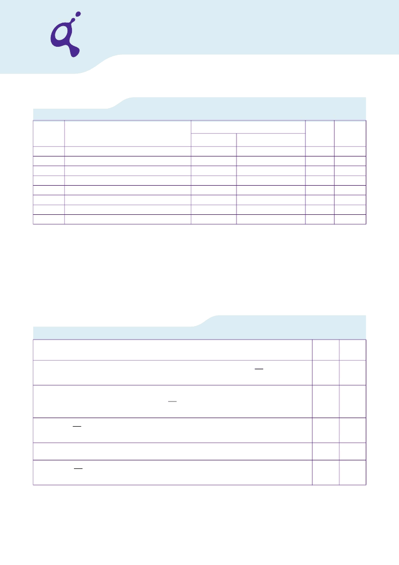
TABLE 16
ODT AC Characteristics and Operating Conditions for DDR2-533 & DDR2-400
3.4
Currents Specifications and Conditions
TABLE 17
I
DD
Measurement Conditions
Symbol
Parameter / Condition
Values
Unit
Note
Min.
Max.
t
AOND
t
AON
t
AONPD
t
AOFD
t
AOF
t
AOFPD
t
ANPD
t
AXPD
ODT turn-on delay
ODT turn-on
ODT turn-on (Power-Down Modes)
ODT turn-off delay
ODT turn-off
ODT turn-off (Power-Down Modes)
ODT to Power Down Mode Entry Latency
ODT Power Down Exit Latency
2
t
AC.MIN
t
AC.MIN
+ 2 ns
2.5
t
AC.MIN
t
AC.MIN
+ 2 ns
3
8
2
t
AC.MAX
+ 1 ns
2
t
CK +
t
AC.MAX
+ 1 ns
2.5
t
AC.MAX
+ 0.6 ns
2.5
t
CK +
t
AC.MAX
+ 1 ns
—
—
t
CK
ns
ns
t
CK
ns
ns
t
CK
t
CK
1)
1) ODT turn on time min. is when the device leaves high impedance and ODT resistance begins to turn on. ODT turn on time max is when
the ODT resistance is fully on. Both are measured from
t
AOND
, which is interpreted differently per speed bin. For DDR2-400/533,
t
AOND
is
10 ns (= 2 x 5 ns) after the clock edge that registered a first ODT HIGH if
t
CK
= 5 ns.
2) ODT turn off time min. is when the device starts to turn off ODT resistance. ODT turn off time max is when the bus is in high impedance.
Both are measured from
t
AOFD
. Both are measured from
t
AOFD
, which is interpreted differently per speed bin. For DDR2-400/533,
t
AOFD
is
12.5 ns (= 2.5 x 5 ns) after the clock edge that registered a first ODT HIGH if
t
CK
= 5 ns.
2)
Parameter
Symbol Note
1)2)3)4)5)6)
Operating Current 0
One bank Active - Precharge;
t
CK
=
t
CK.MIN
,
t
RC
=
t
RC.MIN
,
t
RAS
=
t
RAS.MIN
, CKE is HIGH, CS is HIGH between
valid commands. Address and control inputs are SWITCHING, Databus inputs are SWITCHING.
Operating Current 1
One bank Active - Read - Precharge;
I
OUT
= 0 mA, BL = 4,
t
CK
=
t
CK.MIN
,
t
RC
=
t
RC.MIN
,
t
RAS
=
t
RAS.MIN
,
t
RCD
=
t
RCD.MIN
, AL = 0, CL = CL
MIN
; CKE is HIGH, CS is HIGH between valid commands. Address and
control inputs are SWITCHING, Databus inputs are SWITCHING.
Precharge Standby Current
All banks idle; CS is HIGH; CKE is HIGH;
t
CK
=
t
CK.MIN
; Other control and address inputs are SWITCHING,
Data bus inputs are SWITCHING.
Precharge Power-Down Current
Other control and address inputs are STABLE, Data bus inputs are FLOATING.
Precharge Quiet Standby Current
All banks idle; CS is HIGH; CKE is HIGH;
t
CK
=
t
CK.MIN
; Other control and address inputs are STABLE,
Data bus inputs are FLOATING.
I
DD0
I
DD1
I
DD2N
I
DD2P
I
DD2Q
相關(guān)PDF資料 |
PDF描述 |
|---|---|
| HYS72T128001HR-5-A | 240-Pin Registered DDR SDRAM Modules |
| HYS72T256000HR | 240-Pin Registered DDR SDRAM Modules |
| HYS72T256000HR-3.7-A | 240-Pin Registered DDR SDRAM Modules |
| HYS72T256000HR-3S-A | 240-Pin Registered DDR SDRAM Modules |
| HYS72T256000HR-5-A | 240-Pin Registered DDR SDRAM Modules |
相關(guān)代理商/技術(shù)參數(shù) |
參數(shù)描述 |
|---|---|
| HYS72T128001HR-5-A | 制造商:QIMONDA 制造商全稱:QIMONDA 功能描述:240-Pin Registered DDR SDRAM Modules |
| HYS72T128020EU-2.5-B2 | 制造商:QIMONDA 制造商全稱:QIMONDA 功能描述:240-Pin unbuffered DDR2 SDRAM Modules |
| HYS72T128020EU-25F-B2 | 制造商:QIMONDA 制造商全稱:QIMONDA 功能描述:240-Pin unbuffered DDR2 SDRAM Modules |
| HYS72T128020EU-3.7-B2 | 制造商:QIMONDA 制造商全稱:QIMONDA 功能描述:240-Pin unbuffered DDR2 SDRAM Modules |
| HYS72T128020EU-3-B2 | 制造商:QIMONDA 制造商全稱:QIMONDA 功能描述:240-Pin unbuffered DDR2 SDRAM Modules |
發(fā)布緊急采購,3分鐘左右您將得到回復(fù)。