- 您現(xiàn)在的位置:買賣IC網(wǎng) > PDF目錄370806 > HYS72D128021GR-7-B (INFINEON TECHNOLOGIES AG) Connector Wall Plate; Color:White; Leaded Process Compatible:Yes; No. of Ports:4 RoHS Compliant: Yes PDF資料下載
參數(shù)資料
| 型號: | HYS72D128021GR-7-B |
| 廠商: | INFINEON TECHNOLOGIES AG |
| 英文描述: | Connector Wall Plate; Color:White; Leaded Process Compatible:Yes; No. of Ports:4 RoHS Compliant: Yes |
| 中文描述: | 2.5伏184針注冊的DDR - SDRAM內(nèi)存模塊我 |
| 文件頁數(shù): | 19/23頁 |
| 文件大小: | 418K |
| 代理商: | HYS72D128021GR-7-B |

HYS 72Dxx0xxGR-7/8-B
Registered DDR-I SDRAM-Modules
INFINEON Technologies
19
2002-09-10 (revision 0.91)
APPLICATION NOTE:
Power Up and Power Management on DDR Registered DIMMs
(according to JEDEC ballot JC-42.5 Item 1173)
184-pin Double Data Rate (DDR) Registered DIMMs include two new features to facilitate controlled power-up
and to minimize power consumption during low power mode. One feature is externally controlled via a system-
generated RESET signal
;
the second is based on module detection of the input clocks. These enhancements
permit the modules to power up with SDRAM outputs in a High-
Z
state (eliminating risk of high current dissipa-
tions and
/
or dotted I
/
Os), and result in the powering-down of module support devices (registers and Phase-
Locked Loop) when the memory is in Self-Refresh mode.
The new RESET pin controls power dissipation on the module’s registers and ensures that CKE and other
SDRAM inputs are maintained at a valid ‘low’ level during power-up and self refresh. When RESET is at a low
level, all the register outputs are forced to a low level, and all differential register input receivers are powered
down, resulting in very low register power consumption. The RESET pin, located on DIMM tab
#
10, is driven
from the system as an asynchronous signal according to the attached details. Using this function also permits the
system and DIMM clocks to be stopped during memory Self Refresh operation, while ensuring that the SDRAMs
stay in Self Refresh mode.
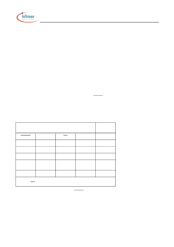
The function for RESET is as follows:
As described in the table above, a low on the RESET input ensures that the Clock Enable (CKE) signal(s) are
maintained low at the SDRAM pins (CKE being one of the
'Q'
signals at the register output). Holding CKE low
maintains a high impedance state on the SDRAM D
Q
, D
Q
S and DM outputs — where they will remain until acti-
vated by a valid ‘read’ cycle. CKE low also maintains SDRAMs in Self Refresh mode when applicable.
The DDR PLL devices automatically detect clock activity above 20MHz. When an input clock frequency of
20MHz or greater is detected, the PLL begins operation and initiates clock frequency lock (the minimum operat-
ing frequency at which all specifications will be met is 95MHz). If the clock input frequency drops below 20MHz
(actual detect frequency will vary by vendor), the PLL VCO (Voltage Controlled Oscillator) is stopped, outputs are
Register Inputs
Register
Outputs
RESET
CK
CK
Data in (D)
Data out (
Q
)
H
Rising
Falling
H
H
H
Rising
Falling
L
L
H
L or H
L or H
X
Q
o
H
High
Z
High
Z
X
Illegal input
conditions
L
X
or Hi-
Z
X
or Hi-
Z
X
or Hi-
Z
L
X
: Don’t care, Hi-
Z
: High Impedance,
Q
o: Data latched at the previous of CK
risning and CK falling
相關(guān)PDF資料 |
PDF描述 |
|---|---|
| HYS72D128021GR-8-B | Connector Wall Plate; Color:Almond; Leaded Process Compatible:Yes; No. of Ports:6 RoHS Compliant: Yes |
| HYS72D64020GR-7-B | 2.5 V 184-pin Registered DDR-I SDRAM Modules |
| HYS72D128020GR-7-A | CONNECTORS, PCB RoHS Compliant: Yes |
| HYS72D64000GR-7-A | TESTPOINT PIN RECEPTACLE |
| HYS72D64020GR-7-A | 2.5 V 184-pin Registered DDR-I SDRAM Modules |
相關(guān)代理商/技術(shù)參數(shù) |
參數(shù)描述 |
|---|---|
| HYS72D128021GR-8-B | 制造商:INFINEON 制造商全稱:Infineon Technologies AG 功能描述:2.5 V 184-pin Registered DDR-I SDRAM Modules |
| HYS72D128300GBR | 制造商:INFINEON 制造商全稱:Infineon Technologies AG 功能描述:184-Pin Registered Double Data Rate SDRAM Module |
| HYS72D128300GBR-5-B | 制造商:INFINEON 制造商全稱:Infineon Technologies AG 功能描述:184-Pin Registered Double Data Rate SDRAM Module |
| HYS72D128300GBR-6-B | 制造商:QIMONDA 制造商全稱:QIMONDA 功能描述:184 - Pin Registered Double-Data-Rate SDRAM Module |
| HYS72D128300GBR-7-B | 制造商:QIMONDA 制造商全稱:QIMONDA 功能描述:184 - Pin Registered Double-Data-Rate SDRAM Module |
發(fā)布緊急采購,3分鐘左右您將得到回復(fù)。