- 您現(xiàn)在的位置:買賣IC網(wǎng) > PDF目錄383076 > HUF75637P3 (INTERSIL CORP) RG8X BULK COAXIAL CABLE PDF資料下載
參數(shù)資料
| 型號(hào): | HUF75637P3 |
| 廠商: | INTERSIL CORP |
| 元件分類: | 功率晶體管 |
| 英文描述: | RG8X BULK COAXIAL CABLE |
| 中文描述: | 44 A, 100 V, 0.03 ohm, N-CHANNEL, Si, POWER, MOSFET, TO-220AB |
| 文件頁數(shù): | 1/9頁 |
| 文件大小: | 332K |
| 代理商: | HUF75637P3 |
1
File Number
4721.1
CAUTION: These devices are sensitive to electrostatic discharge. Follow proper ESD Handling Procedures.
UltraFET is a trademark of Intersil Corporation. PSPICE is a registered trademark of MicroSim Corporation.
SABER
is a Copyright of Analogy Inc. 1-888-INTERSIL or 407-727-9207
|
Copyright
Intersil Corporation 1999.
HUF75637P3, HUF75637S3S
44A, 100V, 0.030 Ohm, N-Channel,
UltraFET Power MOSFET
Packaging
Symbol
Features
Ultra Low On-Resistance
- r
DS(ON)
= 0.030
,
V
GS
=
10V
Simulation Models
- Temperature Compensated PSPICE
and SABER
Electrical Models
- Spice and SABER
Thermal Impedance Models
- www.semi.Intersil.com
Peak Current vs Pulse Width Curve
UIS Rating Curve
Ordering Information
Absolute Maximum Ratings
T
C
= 25
o
C, Unless Otherwise Specified
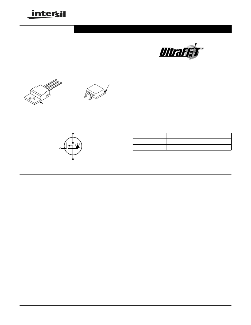
JEDEC TO-220AB
JEDEC TO-263AB
DRAIN
(FLANGE)
GATE
SOURDRAIN
HUF75637P3
GATE
SOURCE
DRAIN
(FLANGE)
HUF75637S3S
D
G
S
PART NUMBER
PACKAGE
BRAND
HUF75637P3
TO-220AB
75637P
HUF75637S3S
TO-263AB
75637S
NOTE: When ordering, use the entire part number. Add the suffix T
to obtain the variant in tape and reel, e.g., HUF75637S3ST.
HUF75637P3, HUF75637S3S
UNITS
Drain to Source Voltage (Note 1). . . . . . . . . . . . . . . . . . . . . . . . . . . . . . . . . . . . . . . . . . V
DSS
Drain to Gate Voltage (R
GS
= 20k
) (Note 1) . . . . . . . . . . . . . . . . . . . . . . . . . . . . . . . .V
DGR
Gate to Source Voltage . . . . . . . . . . . . . . . . . . . . . . . . . . . . . . . . . . . . . . . . . . . . . . . . . . V
GS
Drain Current
Continuous (T
C
= 25
o
C, V
GS
= 10V) (Figure 2) . . . . . . . . . . . . . . . . . . . . . . . . . . . . . . I
D
Continuous (T
C
= 100
o
C, V
GS
= 10V) (Figure 2) . . . . . . . . . . . . . . . . . . . . . . . . . . . . . I
D
Pulsed Drain Current . . . . . . . . . . . . . . . . . . . . . . . . . . . . . . . . . . . . . . . . . . . . . . . . . . .I
DM
Pulsed Avalanche Rating . . . . . . . . . . . . . . . . . . . . . . . . . . . . . . . . . . . . . . . . . . . . . . . . .UIS
100
V
100
V
±
20
V
44
31
Figure 4
A
A
Figures 6, 14, 15
Power Dissipation . . . . . . . . . . . . . . . . . . . . . . . . . . . . . . . . . . . . . . . . . . . . . . . . . . . . . . . P
D
Derate Above 25
o
C . . . . . . . . . . . . . . . . . . . . . . . . . . . . . . . . . . . . . . . . . . . . . . . . . . . . . . .
155
1.03
W
W/
o
C
o
C
Operating and Storage Temperature . . . . . . . . . . . . . . . . . . . . . . . . . . . . . . . . . . . . T
J
, T
STG
Maximum Temperature for Soldering
Leads at 0.063in (1.6mm) from Case for 10s. . . . . . . . . . . . . . . . . . . . . . . . . . . . . . . . . .T
L
Package Body for 10s, See Techbrief TB334. . . . . . . . . . . . . . . . . . . . . . . . . . . . . . . . T
pkg
NOTE:
1. T
J
= 25
o
C to 150
o
C.
CAUTION:
Stresses above those listed in “Absolute Maximum Ratings” may cause permanent damage to the device. This is a stress only rating and operation of the
device at these or any other conditions above those indicated in the operational sections of this specification is not implied.
-55 to 175
300
260
o
C
o
C
Data Sheet
October 1999
相關(guān)PDF資料 |
PDF描述 |
|---|---|
| HUF75637S3S | 44A, 100V, 0.030 Ohm, N-Channel, UltraFET Power MOSFET |
| HUF75637P3 | 44A, 100V, 0.030 Ohm, N-Channel, UltraFET Power MOSFET |
| HUF75637S3S | REPLACEMENT BLADE FOR PTS-10 |
| HUF76107P3 | 20A, 30V, 0.052 Ohm, N-Channel, Logic Level UltraFET Power MOSFETs |
| HUF76107D3 | 20A, 30V, 0.052 Ohm, N-Channel, Logic Level UltraFET Power MOSFETs |
相關(guān)代理商/技術(shù)參數(shù) |
參數(shù)描述 |
|---|---|
| HUF75637P3T | 制造商:未知廠家 制造商全稱:未知廠家 功能描述:TRANSISTOR | MOSFET | N-CHANNEL | 100V V(BR)DSS | 44A I(D) | TO-220AB |
| HUF75637S3 | 制造商:Rochester Electronics LLC 功能描述:- Bulk |
| HUF75637S3_NR4895 | 功能描述:MOSFET 100V 41A 0.03Ohm N-Channel RoHS:否 制造商:STMicroelectronics 晶體管極性:N-Channel 汲極/源極擊穿電壓:650 V 閘/源擊穿電壓:25 V 漏極連續(xù)電流:130 A 電阻汲極/源極 RDS(導(dǎo)通):0.014 Ohms 配置:Single 最大工作溫度: 安裝風(fēng)格:Through Hole 封裝 / 箱體:Max247 封裝:Tube |
| HUF75637S3S | 功能描述:MOSFET 44a 100V 0.030 Ohm N-Ch MOSFET RoHS:否 制造商:STMicroelectronics 晶體管極性:N-Channel 汲極/源極擊穿電壓:650 V 閘/源擊穿電壓:25 V 漏極連續(xù)電流:130 A 電阻汲極/源極 RDS(導(dǎo)通):0.014 Ohms 配置:Single 最大工作溫度: 安裝風(fēng)格:Through Hole 封裝 / 箱體:Max247 封裝:Tube |
| HUF75637S3ST | 功能描述:MOSFET 44a 100V 0.030 Ohm N-Ch MOSFET RoHS:否 制造商:STMicroelectronics 晶體管極性:N-Channel 汲極/源極擊穿電壓:650 V 閘/源擊穿電壓:25 V 漏極連續(xù)電流:130 A 電阻汲極/源極 RDS(導(dǎo)通):0.014 Ohms 配置:Single 最大工作溫度: 安裝風(fēng)格:Through Hole 封裝 / 箱體:Max247 封裝:Tube |
發(fā)布緊急采購,3分鐘左右您將得到回復(fù)。