- 您現(xiàn)在的位置:買賣IC網(wǎng) > PDF目錄371898 > HSP48908VC-32 (HARRIS SEMICONDUCTOR) Two Dimensional Convolver PDF資料下載
參數(shù)資料
| 型號(hào): | HSP48908VC-32 |
| 廠商: | HARRIS SEMICONDUCTOR |
| 元件分類: | 數(shù)字信號(hào)處理外設(shè) |
| 英文描述: | Two Dimensional Convolver |
| 中文描述: | 8-BIT, DSP-CONVOLVER, PQFP100 |
| 文件頁(yè)數(shù): | 6/18頁(yè) |
| 文件大小: | 110K |
| 代理商: | HSP48908VC-32 |
第1頁(yè)第2頁(yè)第3頁(yè)第4頁(yè)第5頁(yè)當(dāng)前第6頁(yè)第7頁(yè)第8頁(yè)第9頁(yè)第10頁(yè)第11頁(yè)第12頁(yè)第13頁(yè)第14頁(yè)第15頁(yè)第16頁(yè)第17頁(yè)第18頁(yè)

6
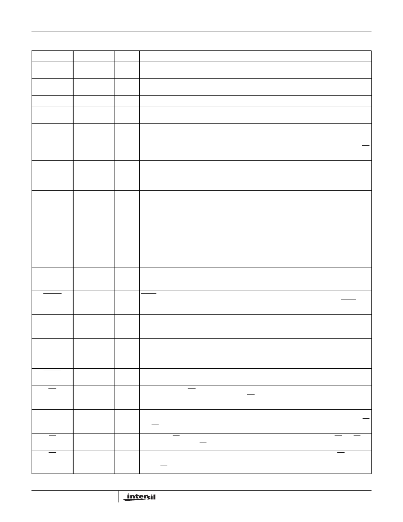
Pin Descriptions
NAME
PLCC PIN
TYPE
DESCRIPTION
V
CC
21, 42, 63, 84
The +5V power supply pins. 0.1
μ
F capacitors between the V
CC
and GND pins are
recommended.
GND
19, 48, 54, 61,
69, 76, 82
The device ground.
CLK
20
I
Input and System Clock. Operations are synchronous with the rising edge of this clock signal.
DIN-07
1-8
I
Pixel Data Input Bus. This bus is used to provide the 8-bit pixel input data to the HSP48908. The
data must be provided in a synchronous fashion, and is latched on the rising edge of the CLK signal.
ClN0-9
9-18
I
Coefficient Input Bus. This input bus is used to load the Coefficient Mask Register(s), the Initializa-
tion Register, the Row Buffer Length Register and the ALU microcode. It may also be used to pro-
vide a second operand input to the ALU. The definition of the ClN0-9 bits is defined by the register
address bits A0-2. The CIN0-9 data is loaded to the Addressed Register through the use of the CS
and LD inputs.
DOUT0-19
49-53, 55-60,
62, 64-68,
70-72
0
Output Data Bus. This 20-Bit output port is used to provide the convolution result. The result is the
sum of products of the input data samples and their corresponding coefficients. The Cascade inputs
CASl0-15 may also be added to the result by selecting the appropriate cascade mode in the Initial-
ization Register.
CASIO-15
29-41, 43-45
I
Cascade Input Bus. This bus is used for cascading multiple HSP48908s to allow convolution with
larger kernels or row sizes. It may also be used to interface to external row buffers. The function of
this bus is determined by the Cascade Mode bit (Bit 0) of the Initialization Register. When this bit is
set to a ‘0’, the value on CASI0-15 is left shifted and added to DOUT0-19. The amount of the shift
is determined by bits 7-8 of the Initialization Register. While this mode is intended primarily for cas-
cading, it may also be used to add an offset value, such as to increase the brightness of the con-
volved image.
When the Cascade mode bit is set to a “1”
,
this bus is used for interfacing to external row buffers.
In this mode the bus is divided into two 8-bit busses (CASl0-7 and CASl8-15), thus allowing two ad-
ditional pixel data inputs. The cascade data is sent directly to the internal multiplier array which al-
lows for larger row sizes without using multiple HSP48908s.
CASO0-7
73-75, 77-81
0
Cascade Output Bus. This bus is used primarily during cascading to handle larger frames and/or
kernel sizes. This output data is the data on DIN0-7 delayed by twice the programmed internal row
buffer length.
FRAME
46
I
Frame is an asynchronous new frame or vertical sync input. A low on this input resets all internal
circuitry except for the Coefficient, ALU, AMC, EOR and INT Registers. Thus, after a Frame reset
has occurred, a new frame of pixels may be convolved without reloading these registers.
EALU
28
I
Enable ALU Input. This control line gates the clock to the ALU Register. When it is high, the data on
CIN0-7 is loaded on the next rising clock edge. When EALU is low, the last value loaded remains in
the ALU Register.
HOLD
22
I
The Hold Input is used to gate the clock from all of the internal circuitry of the H5P48908. This signal
is synchronous, is sampled on the rising edge of CLK and takes effect on the following cycle. While
this signal is active (high), the clock will have no effect on the HSP48908 and
internal data will remain undisturbed.
RESET
47
I
Reset is an asynchronous signal which resets all internal circuitry of the HSP48908. All outputs are
forced low in the reset state.
OE
83
I
Output Enable. The OE input controls the state of the Output Data bus (DOUT0-19). A LOW on this
control line enables the port for output. When OE is HIGH, the output drivers are in the high imped-
ance state. Processing is not interrupted by this pin.
A0-2
25-27
I
Control Register Address. These lines are decoded to determine which register in the control logic
is the destination for the data on the ClN0-9 inputs. Register loading is controlled by the A0-2, LD
and CS inputs.
LD
23
I
Load Strobe. LD is used for loading the Internal Registers of the HSP48908. When CS and LD are
active, the rising edge of LD will latch the CIN0-7 data into the register specified by A0-2.
CS
24
I
Chip Select. The Chip Select input enables loading of the Internal Registers. When CS is low, the
A0-2 address lines are decoded to determine the meaning of the data on the CIN0-7 bus. The rising
edge of LD will then load the Addressed Register.
HSP48908
相關(guān)PDF資料 |
PDF描述 |
|---|---|
| HSP48908883 | Two Dimensional Convolver |
| HSP48908 | Two Dimensional Convolver(兩維卷積器,用于圖形處理和實(shí)時(shí)視頻濾波器) |
| HSP48908GC-20 | Two Dimensional Convolver |
| HSP48908GC-32 | Two Dimensional Convolver |
| HSP50016GC-52 | Digital Down Converter |
相關(guān)代理商/技術(shù)參數(shù) |
參數(shù)描述 |
|---|---|
| HSP4890BVC-20 | 制造商:Rochester Electronics LLC 功能描述:- Bulk |
| HSP-5 | 功能描述:導(dǎo)熱接口產(chǎn)品 Thermal Pad for 3-phase SSR W/Adhsve RoHS:否 制造商:Panasonic Electronic Components 類型:Thermal Graphite Sheets 材料:Graphite Polymer Film 長(zhǎng)度:180 mm 寬度:115 mm 厚度:0.07 mm 工作溫度范圍: |
| HSP50016 | 制造商:INTERSIL 制造商全稱:Intersil Corporation 功能描述:Digital Down Converter |
| HSP50016_00 | 制造商:INTERSIL 制造商全稱:Intersil Corporation 功能描述:Digital Down Converter |
| HSP50016-EV | 制造商:Rochester Electronics LLC 功能描述:HSP50016 EVALUATION PLATFORM - Bulk |
發(fā)布緊急采購(gòu),3分鐘左右您將得到回復(fù)。