- 您現(xiàn)在的位置:買賣IC網(wǎng) > PDF目錄371898 > HSP48410JC-33 (INTERSIL CORP) CONN MEMORY CARD REV BOTTOM PCB PDF資料下載
參數(shù)資料
| 型號: | HSP48410JC-33 |
| 廠商: | INTERSIL CORP |
| 元件分類: | 數(shù)字信號處理外設(shè) |
| 英文描述: | CONN MEMORY CARD REV BOTTOM PCB |
| 中文描述: | 24-BIT, DSP-HISTOGRAM PROCESSOR, PQCC84 |
| 封裝: | PLASTIC, LCC-84 |
| 文件頁數(shù): | 9/12頁 |
| 文件大小: | 84K |
| 代理商: | HSP48410JC-33 |

9
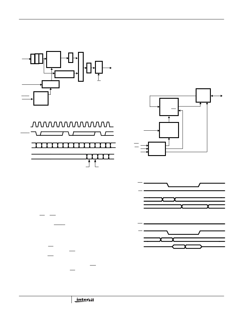
Delay and Subtract Mode
This mode is similar to the Delay Memory mode, except the
input data is subtracted from the corresponding data stored
in RAM (See Figures 12 and 13).
Asynchronous 16/24 Modes
In the Asynchronous modes, the chip acts like a single port
RAM. In this mode, the user can read (access) any bin
location on the fly by simply setting the 10-bit IO address to
the desired bin location. The RAM is then read or written on
the following RD or WR pulse. A block diagram for this mode
is shown in Figure 14. Note that all registers and pipeline
stages are bypassed; START and CLK have no effect in
this mode.
Timing waveforms for this mode are also shown in Figure 15.
During reading, the read address is latched (internally) on
the falling edge of RD. During write operations, the address
is latched on the falling edge of WR and data is latched on
the rising edge of WR. Note that reading and writing occur
on different ports, so that, in this mode, the write port always
latches its address and data values from the WR signal,
while the read port always uses RD for latching.
The difference between the Async 16 mode and the Async
24 mode is the number of data bits available to the user. In
16-bit mode, the user can connect the system data bus to
the lower 16 bits of the Histogrammer’s DIO bus. The UWS
pin becomes the LSB of the IO address, which determines if
the lower 16 bits or upper 8 bits of the 24-bit Histogrammer
data is being used. When UWS is low, the data present at
DIO0-15 is the lower 16 bits of the data in the IOADD0-9
location. When UWS is high, the upper 8 bits of the
IOADD09 location are present on DIO0-7. (This is true for
both reading and writing). Thus, it takes 2 cycles for an
asynchronous 24-bit operation when in Async 16 mode.
Unused outputs are zeros.
RAM
Σ
IN
OUT
ADDRESS
DIO 0-23
CLK
START
CONTROL
DIO
I/F
R
R
COUNTER
R
R
R
DIN 0-23
TWO’S
COMPLEMENT
RD
FIGURE 12. DELAY AND SUBTRACT BLOCK DIAGRAM
CLK
DIN 0-23
START
DIO 0-23
DATA
1
2
3
4
5
6
7
8
9
10 11 12
13
OUTPUT
1
2
3
4
5
MODIFIED DATA
14
DATA 1
MINUS
DATA 7
DATA 2
MINUS
DATA 8
FIGURE 13. DELAY AND SUBTRACT MODE TIMING FOR ROW
LENGTH OF TEN
ADDRESS
GENERATOR
24x1024
RAM
IN
OUT
WR
ADDRESS
DIO 0-23
UWS
CONTROL
DIO
I/F
RD
WR
IOADD 0-9
FIGURE 14. ASYNCHRONOUS 16/24 BLOCK DIAGRAM
WR
IOADD 0-9,
RD
DIO 0-23
READ CYCLE TIMING
WR
IOADD 0-9,
RD
DIO 0-23
WRITE CYCLE TIMING
UWS
UWS
FIGURE 15. ASYNCHRONOUS 16/24 MODE TIMING
HSP48410
相關(guān)PDF資料 |
PDF描述 |
|---|---|
| HSP48410JC-40 | CONN MEMORY CARD NORMAL I/O |
| HSP48901GC-20 | 3 x 3 Image Filter |
| HSP48901GC-30 | 3 x 3 Image Filter |
| HSP48901JC-20 | 3 x 3 Image Filter |
| HSP48901JC-30 | 3 x 3 Image Filter |
相關(guān)代理商/技術(shù)參數(shù) |
參數(shù)描述 |
|---|---|
| HSP48410JC-40 | 制造商:Rochester Electronics LLC 功能描述:HISTOGRAMER 84 PLCC, 40MHZ, COMM - Bulk |
| HSP48901 | 制造商:INTERSIL 制造商全稱:Intersil Corporation 功能描述:3 x 3 Image Filter |
| HSP48901_04 | 制造商:INTERSIL 制造商全稱:Intersil Corporation 功能描述:3 x 3 Image Filter |
| HSP48901GC-20 | 制造商:Rochester Electronics LLC 功能描述:- Bulk |
| HSP48901GC-30 | 制造商:Rochester Electronics LLC 功能描述:- Bulk |
發(fā)布緊急采購,3分鐘左右您將得到回復(fù)。