- 您現(xiàn)在的位置:買賣IC網 > PDF目錄371898 > HSP48410GC-40 (INTERSIL CORP) Histogrammer/Accumulating Buffer PDF資料下載
參數(shù)資料
| 型號: | HSP48410GC-40 |
| 廠商: | INTERSIL CORP |
| 元件分類: | 數(shù)字信號處理外設 |
| 英文描述: | Histogrammer/Accumulating Buffer |
| 中文描述: | 24-BIT, DSP-HISTOGRAM PROCESSOR, CPGA84 |
| 封裝: | PGA-84 |
| 文件頁數(shù): | 5/12頁 |
| 文件大?。?/td> | 84K |
| 代理商: | HSP48410GC-40 |

5
Functional Description
The Histogrammer is intended for use in signal and image
processing applications. The on-board RAM is 24 bits by
1024 locations. For histogramming, this translates to an
image size of 4k x 4k with 10-bit data. A Functional Block
Diagram of the part is shown in Figure 1.
In addition to histogramming, the HSP48410 will also
perform Histogram Accumulation while feeding the results
back into the memory array. The on-board RAM will then
contain the Cumulative Distribution Function and can be
used for further operation such as histogram equalization.
Other modes are: Bin Accumulate, Look Up Table (LUT),
Delay Memory, and Delay and Subtract. The part can also
be accessed as a 24-bit by 1024 word asynchronous RAM
for preconditioning or reading the results of the histogram.
The Histogrammer can be accessed both synchronously
and asynchronously to the system clock (CLK). It was
designed to be configured asynchronously by a
microprocessor, then switched to a synchronous mode to
process data. The result of the processing can then be read
out synchronously, or the part can be switched to one of the
asynchronous modes so the data may be read out by a
microprocessor. All modes are synchronous except for the
Asynchronous 16 and 24 modes.
A Flash Clear operation allows the user to reset the entire
RAM array and all input and output data paths in a single
cycle.
Histogram Memory Array
The Histogram Memory Array is a 24-bit by 1024 deep RAM.
Depending on the current mode, its input data comes from
either the synchronous input DIN0-23, from the
asynchronous data bus DIO0-23, or from the output of the
adder. The output data goes to the DIO bus in both
synchronous and asynchronous modes.
Address Generator
This section of the circuit determines the source of the RAM
address. In the synchronous modes, the address is taken
from either the output of the counter or PIN0-9. The pixel
input bus is used for Histogram, Bin Accumulate, and
LUT(read) modes. All other synchronous modes, i.e.
Histogram Accumulate, LUT(write), Delay, and Delay and
Subtract use the counter output. The counter is reset on the
first rising edge of CLK after a falling edge on START.
During asynchronous modes, the read and write addresses
to the RAM are taken from the IOADD bus on the falling
edge of the RD and WR signals, respectively.
Adder Input
The Adder Input Control Section contains muxes, registers
and other logic that provide the proper data to the adder. The
configuration of this section is controlled by the output of the
Function Decode Section.
DIO Interface
The DIO Interface Section transfers data between the
Histogrammer and the outside world. In the synchronous
modes, DIO acts as a synchronous output for the data
currently being processed by the chip; RD acts as the output
enable for the DIO bus; WR and IOADD0-9 have no effect.
When either of the Asynchronous modes are selected (16 or
24-bit), the RAM output is passed directly to the DIO bus on
read cycles, and on write cycles, data input on DIO goes to
the RAM input port. In this case, data reads and writes are
controlled by RD, WR and IOADD0-9.
Function Decode
This section provides the signals needed to configure the
part for the different modes. The eight modes are decoded
from FCT0-2 on the rising edge of LD (see Table 1). The
output of this section is a set of signals which control the
path of data through the part.
The mode should only be changed while START is high.
After changing from one mode to another, START must be
clocked high by the rising edge of CLK at least once.
Flash Clear
Flash Clear allows the user to clear the entire RAM with a
single pin. When the FC pin is low, all bits of the RAM and
the data path from the RAM to DIO0-23 are set to zero. The
FC pin is asynchronous with respect to CLK: the reset
begins immediately following a low on this signal. For
synchronous modes, in order to ensure consistent results,
FC should only be active while START is high. For
asynchronous modes, WR must remain inactive while FC
is low.
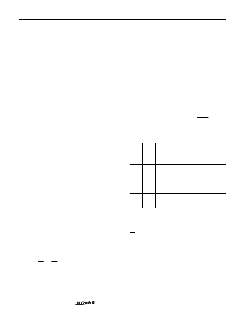
TABLE 1. FUNCTION DECODE
FCT
MODE
2
1
0
0
0
0
Histogram
0
0
1
Histogram Accumulate
0
1
0
Delay and Subtract
0
1
1
Look Up Table
1
0
0
Bin Accumulate
1
0
1
Delay Memory
1
1
0
Asynchronous 24
1
1
1
Asynchronous 16
HSP48410
相關PDF資料 |
PDF描述 |
|---|---|
| HSP48410 | Histogrammer/Accumulating Buffer |
| HSP48410883 | Histogrammer/Accumulating Buffer |
| HSP48410JC-33 | CONN MEMORY CARD REV BOTTOM PCB |
| HSP48410JC-40 | CONN MEMORY CARD NORMAL I/O |
| HSP48901GC-20 | 3 x 3 Image Filter |
相關代理商/技術參數(shù) |
參數(shù)描述 |
|---|---|
| HSP48410GM-25/883 | 制造商:Rochester Electronics LLC 功能描述:- Bulk |
| HSP48410GM-33/883 | 制造商:INTERSIL 制造商全稱:Intersil Corporation 功能描述:Histogrammer/Accumulating Buffer |
| HSP48410JC-33 | 制造商:Rochester Electronics LLC 功能描述:HISTOGRAMER 84 PLCC, 33MHZ, COMM - Bulk |
| HSP48410JC-40 | 制造商:Rochester Electronics LLC 功能描述:HISTOGRAMER 84 PLCC, 40MHZ, COMM - Bulk |
| HSP48901 | 制造商:INTERSIL 制造商全稱:Intersil Corporation 功能描述:3 x 3 Image Filter |
發(fā)布緊急采購,3分鐘左右您將得到回復。