- 您現(xiàn)在的位置:買賣IC網(wǎng) > PDF目錄370698 > HSMS-2822-TR1 Surface Mount RF Schottky Barrier Diodes PDF資料下載
參數(shù)資料
| 型號: | HSMS-2822-TR1 |
| 英文描述: | Surface Mount RF Schottky Barrier Diodes |
| 中文描述: | 表面貼裝射頻肖特基二極管 |
| 文件頁數(shù): | 5/14頁 |
| 文件大小: | 209K |
| 代理商: | HSMS-2822-TR1 |

Applications Information
Product Selection
Agilent’s family of surface mount
Schottky diodes provide unique
solutions to many design prob-
lems. Each is optimized for
certain applications.
The first step in choosing the right
product is to select the diode type.
All of the products in the
HSMS-282x family use the same
diode chip–they differ only in
package configuration. The same
is true of the HSMS-280x, -281x,
285x, -286x and -270x families.
Each family has a different set of
characteristics, which can be
compared most easily by consult-
ing the SPICE parameters given
on each data sheet.
The HSMS-282x family has been
optimized for use in RF applica-
tions, such as
DC biased small signal
detectors to 1.5 GHz.
Biased or unbiased large
signal detectors (AGC or
power monitors) to 4 GHz.
Mixers and frequency
multipliers to 6 GHz.
The other feature of the
HSMS-282x family is its
unit-to-unit and lot-to-lot consis-
tency. The silicon chip used in this
series has been designed to use
the fewest possible processing
steps to minimize variations in
diode characteristics. Statistical
data on the consistency of this
product, in terms of SPICE
parameters, is available from
Agilent.
For those applications requiring
very high breakdown voltage, use
the HSMS-280x family of diodes.
Turn to the HSMS-281x when you
need very low flicker noise. The
HSMS-285x is a family of zero bias
detector diodes for small signal
applications. For high frequency
detector or mixer applications,
use the HSMS-286x family. The
HSMS-270x is a series of specialty
diodes for ultra high speed
clipping and clamping in digital
circuits.
Schottky Barrier Diode
Characteristics
Stripped of its package, a
Schottky barrier diode chip
consists of a metal-semiconductor
barrier formed by deposition of a
metal layer on a semiconductor.
The most common of several
different types, the passivated
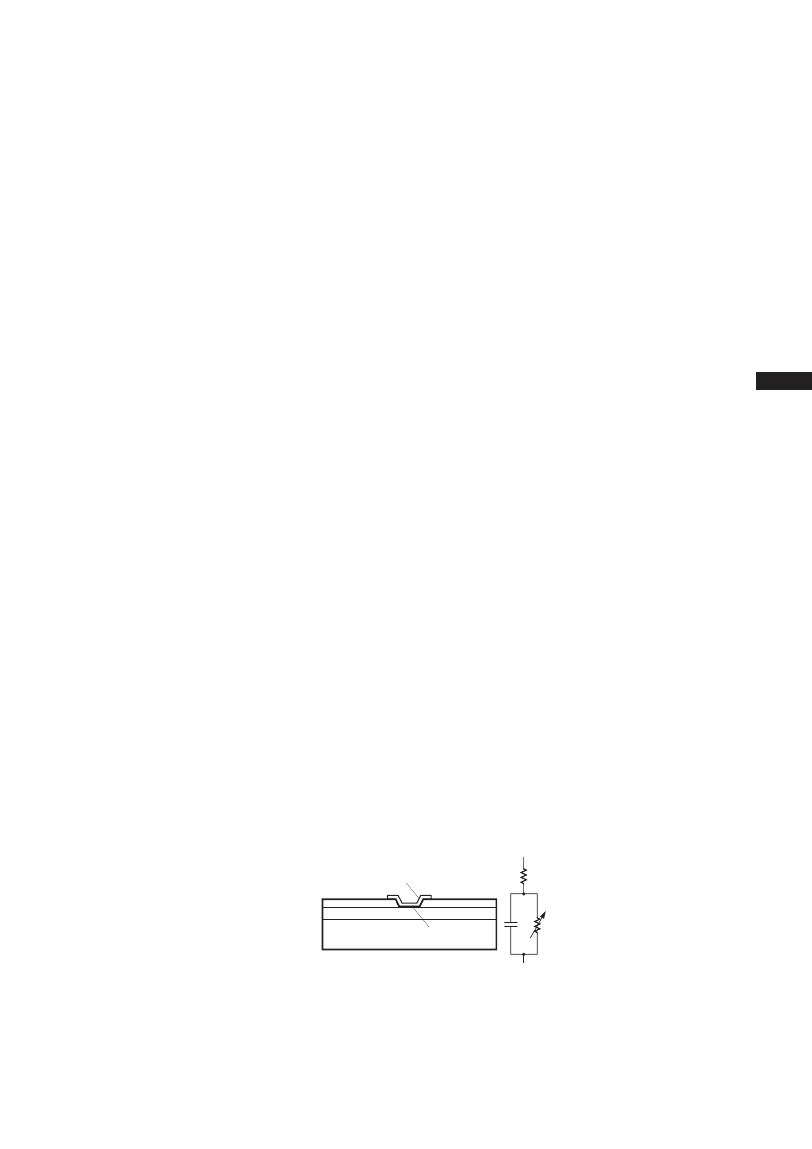
diode, is shown in Figure 10,
along with its equivalent circuit.
R
S
is the parasitic series resis-
tance of the diode, the sum of the
bondwire and leadframe resis-
tance, the resistance of the bulk
layer of silicon, etc. RF energy
coupled into R
S
is lost as heat—it
does not contribute to the recti-
fied output of the diode. C
J
is
parasitic junction capacitance of
the diode, controlled by the thick-
ness of the epitaxial layer and the
diameter of the Schottky contact.
R
j
is the junction resistance of the
diode, a function of the total
current flowing through it.
R
S
R
j
C
j
METAL
SCHOTTKY JUNCTION
PASSIVATION
N-TYPE OR P-TYPE EPI LAYER
PASSIVATION
N-TYPE OR P-TYPE SILICON SUBSTRATE
CROSS-SECTION OF SCHOTTKY
BARRIER DIODE CHIP
EQUIVALENT
CIRCUIT
8.33 X 10
-5
nT
R
j
= –––––––––––– = R
V
– R
s
I
S
+ I
b
0.026
––––– at 25
°
C
I
S
+ I
b
where
n = ideality factor (see table of
SPICE parameters)
T = temperature in
°
K
I
S
= saturation current (see
table of SPICE parameters)
I
b
= externally applied bias
current in amps
R
v
= sum of junction and series
resistance, the slope of the
V-I curve
I
S
is a function of diode barrier
height, and can range from
picoamps for high barrier diodes
to as much as 5
μ
A for very low
barrier diodes.
The Height of the Schottky
Barrier
The current-voltage characteristic
of a Schottky barrier diode at
room temperature is described by
the following equation:
S
0.026
I = I
S
(e –––––– 1)
On a semi-log plot (as shown in
the Agilent catalog) the current
graph will be a straight line with
inverse slope 2.3 X 0.026 = 0.060
volts per cycle (until the effect of
Figure 10. Schottky Diode Chip.
相關(guān)PDF資料 |
PDF描述 |
|---|---|
| HSMS-2822-TR2 | Surface Mount RF Schottky Barrier Diodes |
| HSMS-2820-BLK | Surface Mount RF Schottky Barrier Diodes |
| HSMS-2820-TR1 | Surface Mount RF Schottky Barrier Diodes |
| HSMS-2820-TR2 | Surface Mount RF Schottky Barrier Diodes |
| HSMS-2823-BLK | Surface Mount RF Schottky Barrier Diodes |
相關(guān)代理商/技術(shù)參數(shù) |
參數(shù)描述 |
|---|---|
| HSMS-2822-TR1G | 功能描述:肖特基二極管與整流器 15 VBR 1 pF RoHS:否 制造商:Skyworks Solutions, Inc. 產(chǎn)品:Schottky Diodes 峰值反向電壓:2 V 正向連續(xù)電流:50 mA 最大浪涌電流: 配置:Crossover Quad 恢復時間: 正向電壓下降:370 mV 最大反向漏泄電流: 最大功率耗散:75 mW 工作溫度范圍:- 65 C to + 150 C 安裝風格:SMD/SMT 封裝 / 箱體:SOT-143 封裝:Reel |
| HSMS2822TR2 | 制造商:H.P. 功能描述:HP SMT DIODE |
| HSMS-2822-TR2 | 制造商:AGILENT 制造商全稱:AGILENT 功能描述:Surface Mount RF Schottky Barrier Diodes |
| HSMS-2822-TR2G | 功能描述:肖特基二極管與整流器 15 VBR 1 pF RoHS:否 制造商:Skyworks Solutions, Inc. 產(chǎn)品:Schottky Diodes 峰值反向電壓:2 V 正向連續(xù)電流:50 mA 最大浪涌電流: 配置:Crossover Quad 恢復時間: 正向電壓下降:370 mV 最大反向漏泄電流: 最大功率耗散:75 mW 工作溫度范圍:- 65 C to + 150 C 安裝風格:SMD/SMT 封裝 / 箱體:SOT-143 封裝:Reel |
| HSMS2823 | 制造商:未知廠家 制造商全稱:未知廠家 功能描述:Surface Mount Zero Bias Schottky |
發(fā)布緊急采購,3分鐘左右您將得到回復。