- 您現(xiàn)在的位置:買賣IC網(wǎng) > PDF目錄371885 > HS9-565ARH (HARRIS SEMICONDUCTOR) Radiation Hardened High Speed, Monolithic Digital-to-Analog Converter PDF資料下載
參數(shù)資料
| 型號: | HS9-565ARH |
| 廠商: | HARRIS SEMICONDUCTOR |
| 元件分類: | DAC |
| 英文描述: | Radiation Hardened High Speed, Monolithic Digital-to-Analog Converter |
| 中文描述: | PARALLEL, WORD INPUT LOADING, 0.35 us SETTLING TIME, 12-BIT DAC, CQFP24 |
| 文件頁數(shù): | 4/7頁 |
| 文件大小: | 169K |
| 代理商: | HS9-565ARH |

4
Power Supply Sensitivity
Power Supply Sensitivity is a measure of the change in gain
and offset of the D/A converter resulting from a change in -
15V or +15V supplies. It is specified under DC conditions
and expressed as parts per million of full scale range per
percent of change in power supply (ppm of FSR/%).
Compliance
Compliance Voltage is the maximum output voltage range
that can be tolerated and still maintain its specified accuracy.
Compliance Limit implies functional operation only and
makes no claims to accuracy.
Glitch
A glitch on the output of a D/A converter is a transient spike
resulting from unequal internal ON-OFF switching times.
Worst case glitches usually occur at half scale or the major
carry code transition from 011 . . . 1 to 100 . . . 0 or vice
versa. For example, if turn ON is greater than turn OFF for
011 . . . 1 to 100 . . . 0, an intermediate state of 000 . . . 0
exists, such that, the output momentarily glitches toward
zero output. Matched switching times and fast switching will
reduce glitches considerably.
Applying the HS-565BRH
OP AMP Selection
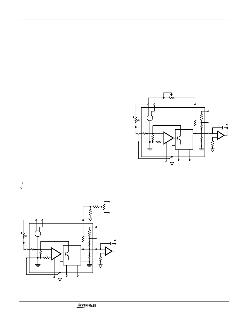
The HS-565BRH’s current output may be converted to
voltage using the standard connections shown in Figures 1
and 2. The choice of operational amplifier should be
reviewed for each application, since a significant trade-off
may be made between speed and accuracy. Remember
settling time for the DAC-amplifier combination is
)
2
tA
where t
D
, t
A
are settling times for the DAC and amplifier.
No Trim Operation
The HS-565BRH will perform as specified without calibration
adjustments. To operate without calibration, substitute 50
resistors for the 100
trimming potentiometers: In Figure 1
replace R2 with 50
; also remove the network on pin 8 and
connect 50
to ground. For bipolar operation in Figure 2,
replace R3 and R4 with 50
resistors.
With these changes, performance is guaranteed as shown
under Specifications, “External Adjustments”. Typical
unipolar zero will be
±
0.50
LSB plus the op amp offset.
The feedback capacitor C must be selected to minimize
settling time.
Calibration
Calibration provides the maximum accuracy from a
converter by adjusting its gain and offset errors to zero, For
the HS-565BRH, these adjustments are similar whether the
current output is used, or whether an external op amp is
added to convert this current to a voltage. Refer to Table 7
for the voltage output case, along with Figure 1 or 2.
Calibration is a two step process for each of the five output
ranges shown in Table 7. First adjust the negative full scale
(zero for unipolar ranges). This is an offset adjust which
translates the output characteristic, i.e. affects each code by
the same amount.
Next adjust positive FS. This is a gain error adjustment, which
rotates the output characteristic about the negative FS value.
For the bipolar ranges, this approach leaves an error at the
zero code, whose maximum values is the same as for
integral nonlinearity error. In general, only two values of
output may be calibrated exactly; all others must tolerate
some error. Choosing the extreme end points (plus and
minus full scale) minimizes this distributed error for all other
codes.
tD
(
(
)
2
+
VO
-
+
R (SEE
TABLE 7)
DAC
OUT
9
10
11
20V SPAN
10V SPAN
2.5K
5K
5K
C
9.95K
IO
24
MSB
13
LSB
. . . . .
CODE
INPUT
DAC
(4 x IREF
x CODE)
-VEE
PWR
7
IREF
0.5mA
HS-565BRH
3K
3.5K
19.95
K
+
-
10V
3
4
VCC
+
-
6
5
REF
GND
REF
IN
REF OUT
R2
100
8
BIP.
OFF.
+15V
-15V
R1
50k
100k
100
FIGURE 1. UNIPOLAR VOLTAGE OUTPUT
VO
-
+
R (SEE
TABLE 7)
DAC
OUT
9
10
11
20V SPAN
10V SPAN
2.5K
5K
5K
C
9.95K
IO
24
13
LSB
MSB
. . . . .
CODE
INPUT
DAC
(4 x IREF
x CODE)
-VEE
PWR
7
IREF
0.5mA
HS-565BRH
3K
3.5K
19.95K
+
-
10V
3
4
VCC
+
-
6
5
REF
GND
REF
IN
REF OUT
R4
100
8
BIP.
OFF.
R3
100
FIGURE 2. BIPOLAR VOLTAGE OUTPUT
HS-565BRH
相關(guān)PDF資料 |
PDF描述 |
|---|---|
| HS9-565ARH-T | Radiation Hardened High Speed, Monolithic Digital-to-Analog Converter |
| HS0-9008RH-Q | Radiation Hardened CMOS 8-Bit Flash Analog-to-Digital Converter |
| HS9-9008RH | Radiation Hardened CMOS 8-Bit Flash Analog-to-Digital Converter |
| HS1-9008RH | Radiation Hardened CMOS 8-Bit Flash Analog-to-Digital Converter |
| HS-9008RH | CMOS 8-Bit Flash Analog-to-Digital Converter(CMOS8位帶Flash存儲器的A/D轉(zhuǎn)換器) |
相關(guān)代理商/技術(shù)參數(shù) |
參數(shù)描述 |
|---|---|
| HS9-565ARH/PROTO | 制造商:INTERSIL 制造商全稱:Intersil Corporation 功能描述:Radiation Hardened High Speed, Monolithic Digital-to-Analog Converter |
| HS9-565ARH-Q | 制造商:未知廠家 制造商全稱:未知廠家 功能描述:12-Bit Digital-to-Analog Converter |
| HS9-565ARH-T | 制造商:INTERSIL 制造商全稱:Intersil Corporation 功能描述:Radiation Hardened High Speed, Monolithic Digital-to-Analog Converter |
| HS9-565BEH-Q | 制造商:Intersil Corporation 功能描述:RAD HARD 12 BIT D/A CONVERTER, FLATPACK, CLS V, HDR/LDR - Trays |
| HS9-565BRH/PROTO | 制造商:Intersil Corporation 功能描述:DAC 1CH R-2R 12-BIT 24CFPAK - Bulk |
發(fā)布緊急采購,3分鐘左右您將得到回復(fù)。