- 您現(xiàn)在的位置:買賣IC網(wǎng) > PDF目錄370684 > HS3160C-4Q 16-Bit Multiplying DACs PDF資料下載
參數(shù)資料
| 型號(hào): | HS3160C-4Q |
| 英文描述: | 16-Bit Multiplying DACs |
| 中文描述: | 16位乘法數(shù)模轉(zhuǎn)換器 |
| 文件頁(yè)數(shù): | 4/8頁(yè) |
| 文件大?。?/td> | 130K |
| 代理商: | HS3160C-4Q |

Corporation
SIGNAL PROCESSING EXCELLENCE
130
PIN ASSIGNMENTS
HS3160 22–PIN
Pin 1 – IO
1
– Current Output 1.
Pin 2 – IO
2
– Current Output 2.
Pin 3 – GND – Ground.
Pin 4 – DB
15
– MSB, Data Bit 1.
Pin 5 – DB
14
– Data Bit 2.
Pin 6 – DB
13
– Data Bit 3.
Pin 7 – DB
12
– Data Bit 4.
Pin 8 – DB
11
– Data Bit 5.
Pin 9 – DB
10
– Data Bit 6.
Pin 10 – DB
9
– Data Bit 7.
Pin 11 – DB
8
– Data Bit 8.
Pin 12 – DB
7
– Data Bit 9.
Pin 13 – DB
6
– Data Bit 10.
Pin 14 – DB
5
– Data Bit 11.
Pin 15 – DB
4
– Data Bit 12.
Pin 16 – DB
3
– Data Bit 13.
Pin 17 – DB
2
– Data Bit 14.
Pin 18 – DB
1
– Data Bit 15.
Pin 19 – DB
0
– LSB, Data Bit 16.
Pin 20 – V
DD
– Positive Supply Voltage.
Pin 21 – V
REF
– Reference Voltage Input.
Pin 22 – R
FB
– Feedback Resistor.
SP7516 24–PIN
Pin 1 – IO
1
– Current Output 1.
Pin 2 – IO
2
Sense – Current Output 2.
Pin 3 – IO
3
Force – Current Output 3.
Pin 4 – GND – Ground.
Pin 5 – DB
15
– MSB, Data Bit 1.
Pin 6 – DB
14
– Data Bit 2.
Pin 7 – DB
13
– Data Bit 3.
Pin 8 – DB
12
– Data Bit 4.
Pin 9 – DB
11
– Data Bit 5.
Pin 10 – DB
10
– Data Bit 6.
Pin 11 – DB
9
– Data Bit 7.
Pin 12 – DB
8
– Data Bit 8.
Pin 13 – DB
7
– Data Bit 9.
Pin 14 – DB
6
– Data Bit 10.
Pin 15 – DB
5
– Data Bit 11.
Pin 16 – DB
4
– Data Bit 12.
Pin 17 – DB
3
– Data Bit 13.
Pin 18 – DB
2
– Data Bit 14.
Pin 19 – DB
1
– Data Bit 15.
Pin 20 – DB
0
– LSB, Data Bit 16.
Pin 21 – V
DD
– Positive Supply Voltage.
Pin 22 – V
REF
Sense – Reference Voltage Input.
Pin 23 – V
REF
Force – Reference Voltage Input.
Pin 24 – R
FB
– Feedback Resistor.
FEATURES…
The
SP7516
and
HS3160
are precision 16-bit multi-
plying DACs. The DACs are implemented as a one-
chip CMOS circuit with a resistor ladder network.
Three output lines are provided on the DACs to allow
unipolar and bipolar output connection with a mini-
mum of external components. The feedback resistor
is internal. The resistor ladder network termination is
externally available, thus eliminating an external re-
sistor for the 1 LSB offset in bipolar mode.
The
SP7516
is available for use in commercial and
industrial temperature ranges, packaged in a 24-pin
SOIC. The
HS3160
is available in commercial
and military temperature ranges, packaged in a
24–pin side–brazed DIP. For product processed
and screened to the requirements of MIL–M–
38510 and MIL–STD–883C, please consult the
factory (
HS3160B
only).
PRINCIPLES OF OPERATION
The
SP7516/HS3160
achieve high accuracy by using
a decoded or segmented DAC scheme to implement
this function. The following is a brief description of
this approach.
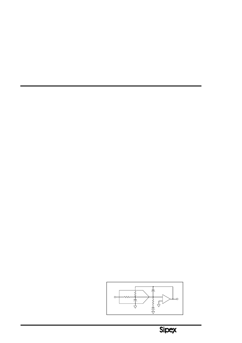
Figure 1. SP7516/HS3160 Equivalent Output Circuit
+
–
EO
Cf
C
Rp
Rf
CO
Ri
VREF
相關(guān)PDF資料 |
PDF描述 |
|---|---|
| HS7516 | 16-Bit Multiplying DACs |
| HS326-SERIES | Peripheral IC |
| HS336-SERIES | Peripheral IC |
| HS3300 | Peripheral IC |
| HS33806 | 12-Bit Digital-to-Analog Converter |
相關(guān)代理商/技術(shù)參數(shù) |
參數(shù)描述 |
|---|---|
| HS-317 | 制造商:Hozan Tool Industrial 功能描述:aF1.0mm t[n_PDO^WOO Bulk |
| HS-317C | 制造商:DFI-ITOX 功能描述:CPU FAN/HEATSINK |
| HS-3182 | 制造商:INTERSIL 制造商全稱:Intersil Corporation 功能描述:ARINC 429 Bus Interface Line Driver Circuit |
| HS-3182_07 | 制造商:INTERSIL 制造商全稱:Intersil Corporation 功能描述:ARINC 429 Bus Interface Line Driver |
| HS32 | 功能描述:散熱片 Heatsink, SIP,Single In Line Pkg RoHS:否 制造商:Ampro By ADLINK 產(chǎn)品:Heat Sink Accessories 安裝風(fēng)格:Through Hole 散熱片材料: 散熱片樣式: 熱阻: 長(zhǎng)度: 寬度: 高度: 設(shè)計(jì)目的:Express-HRR |
發(fā)布緊急采購(gòu),3分鐘左右您將得到回復(fù)。