- 您現(xiàn)在的位置:買賣IC網(wǎng) > PDF目錄371882 > HPW7095A (Electronic Theatre Controls, Inc.) 6-Channel DC/DC Converter Control IC PDF資料下載
參數(shù)資料
| 型號(hào): | HPW7095A |
| 廠商: | Electronic Theatre Controls, Inc. |
| 英文描述: | 6-Channel DC/DC Converter Control IC |
| 中文描述: | 6通道DC / DC變換器控制IC |
| 文件頁(yè)數(shù): | 18/23頁(yè) |
| 文件大小: | 350K |
| 代理商: | HPW7095A |
第1頁(yè)第2頁(yè)第3頁(yè)第4頁(yè)第5頁(yè)第6頁(yè)第7頁(yè)第8頁(yè)第9頁(yè)第10頁(yè)第11頁(yè)第12頁(yè)第13頁(yè)第14頁(yè)第15頁(yè)第16頁(yè)第17頁(yè)當(dāng)前第18頁(yè)第19頁(yè)第20頁(yè)第21頁(yè)第22頁(yè)第23頁(yè)
Rev. A.2 - J uly., 2004
HPW 7095/ A
18
Copyright
HIPAC Semiconductor, Inc.
www.hipacsemi.com
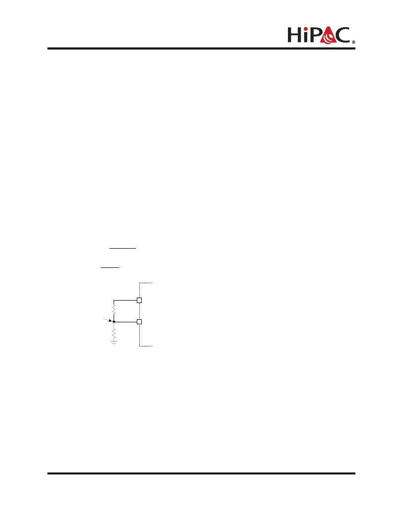
Application Information (Cont.)
Dead-Time Setting
The dead-time control pin (DTC) is designed to set
the maximum ON duty of the main-side MOSFET.
When the device is set for step-up inverted output based
on the step-up or step-up/down Zeta method or flyback
method, the FB pin voltage may reach and exceed
the triangular wave voltage due to load fluctuation. If
this is the case, the output MOSFET is fixed to a ON
duty of 100 %. To prevent this, set the maximum duty
of the output MOSFET. Connecting a resistor- divider
between VREF, DTC and GND pins provides a volt-
age V
DTC
to DTC pin. When the the voltage at the
DTC pin is higher than the triangular wave voltage (CT1/
2), the output transistor is turned on. The maximum
duty is calculated as the following equation:
DTC1
VREF
R1
R2
V
DTC
(%)
100
V
0.7
V
1.1
-
V
Duty
ON
DTC
(max)
=
REF
DTC
V
R2
R1
R2
+
(V)
V
=
where V
REF
is the output of the reference voltage (2.
49V typical) at VREF pin. The amplitude of the trian-
gular waves CT1 and CT2 are typically 0.7V from 1.
1V to 1.8V.
相關(guān)PDF資料 |
PDF描述 |
|---|---|
| HQV101 | Analog IC |
| HR1023 | Analog IC |
| HR1060 | ASIC |
| HR1155PAS | |
| HR1156PAS | |
相關(guān)代理商/技術(shù)參數(shù) |
參數(shù)描述 |
|---|---|
| HPW70C19X30E | 制造商:Hubbell Premise Wiring 功能描述: |
| HPW78C19X30 | 制造商:Hubbell Premise Wiring 功能描述: |
| HPW78C19X30E | 制造商:Hubbell Premise Wiring 功能描述: |
| HPW78C19X30EB | 制造商:Hubbell Premise Wiring 功能描述: |
| HPW78C19X30ET | 制造商:Hubbell Premise Wiring 功能描述: |
發(fā)布緊急采購(gòu),3分鐘左右您將得到回復(fù)。