- 您現(xiàn)在的位置:買賣IC網(wǎng) > PDF目錄371830 > HM1-6518883 (Intersil Corporation) 1024 x 1 CMOS RAM PDF資料下載
參數(shù)資料
| 型號(hào): | HM1-6518883 |
| 廠商: | Intersil Corporation |
| 英文描述: | 1024 x 1 CMOS RAM |
| 中文描述: | 1024 × 1 CMOS存儲(chǔ)器 |
| 文件頁數(shù): | 1/9頁 |
| 文件大小: | 220K |
| 代理商: | HM1-6518883 |
6-85
March 1997
HM-6518/883
1024 x 1 CMOS RAM
Features
This Circuit is Processed in Accordance to MIL-STD-
883 and is Fully Conformant Under the Provisions of
Paragraph 1.2.1.
Low Power Standby. . . . . . . . . . . . . . . . . . . . 50
μ
W Max
Low Power Operation . . . . . . . . . . . . . 20mW/MHz Max
Fast Access Time. . . . . . . . . . . . . . . . . . . . . .180ns Max
Data Retention . . . . . . . . . . . . . . . . . . . . . . . .at 2.0V Min
TTL Compatible Input/Output
High Output Drive - 2 TTL Loads
High Noise Immunity
On-Chip Address Register
Two-Chip Selects for Easy Array Expansion
Three-State Output
Description
The HM-6518/883 is a 1024 x 1 static CMOS RAM
fabricated using self-aligned silicon gate technology.
Synchronous circuit design techniques are employed to
achieve high performance and low power operation.
On chip latches are provided for address and data outputs
allowing efficient interfacing with microprocessor systems.
The data output buffers can be forced to a high impedance
state for use in expanded memory arrays.
The HM-6518/883 is a fully static RAM and may be
maintained in any state for an indefinite period of time. Data
retention supply voltage and supply current are guaranteed
over temperature.
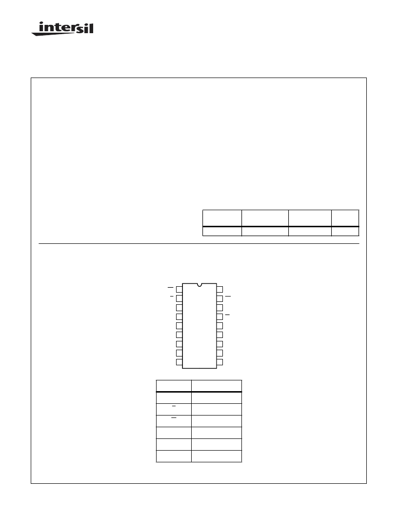
Pinout
HM-6518/883
(CERDIP)
TOP VIEW
Ordering Information
PACKAGE
TEMP. RANGE
-55
o
C to +125
o
C
PART
NUMBER
PKG. NO.
CERDIP
HM1-6518/883
F18.3
PIN
DESCRIPTION
A
Address Input
E
Chip Enable
W
Write Enable
S
Chip Select
D
Data Input
Q
Data Output
10
11
12
13
14
15
16
17
18
9
8
7
6
5
4
3
2
1
VCC
D
W
A9
A8
A7
A6
S2
A5
S1
E
A0
A1
A2
A3
Q
A4
GND
File Number
2986.1
CAUTION: These devices are sensitive to electrostatic discharge; follow proper IC Handling Procedures.
http://www.intersil.com or 407-727-9207
|
Copyright
Intersil Corporation 1999
相關(guān)PDF資料 |
PDF描述 |
|---|---|
| HM-65262 | 16K x 1 Asynchronous CMOS Static RAM |
| HM-65262883 | 16K x 1 Asynchronous CMOS Static RAM |
| HM1-65262-9 | 16K x 1 Asynchronous CMOS Static RAM |
| HM1-65262B-9 | 16K x 1 Asynchronous CMOS Static RAM |
| HM-6551B883 | 256 x 4 CMOS RAM |
相關(guān)代理商/技術(shù)參數(shù) |
參數(shù)描述 |
|---|---|
| HM1-6518-9 | 制造商:Rochester Electronics LLC 功能描述:- Bulk |
| HM1-6518B | 制造商:Rochester Electronics LLC 功能描述:- Bulk |
| HM1-6518B/883 WAF | 制造商:Harris Corporation 功能描述: |
| HM1-6518B1390-501B | 制造商:Rochester Electronics LLC 功能描述:- Bulk |
| HM1-6518B-9 | 制造商:Rochester Electronics LLC 功能描述:- Bulk |
發(fā)布緊急采購,3分鐘左右您將得到回復(fù)。