- 您現(xiàn)在的位置:買賣IC網(wǎng) > PDF目錄383058 > HIP6021EVAL1 (Intersil Corporation) Advanced PWM and Triple Linear Power Controller PDF資料下載
參數(shù)資料
| 型號: | HIP6021EVAL1 |
| 廠商: | Intersil Corporation |
| 元件分類: | 基準(zhǔn)電壓源/電流源 |
| 英文描述: | Advanced PWM and Triple Linear Power Controller |
| 中文描述: | 先進(jìn)的PWM和三線性功率控制器 |
| 文件頁數(shù): | 4/16頁 |
| 文件大小: | 186K |
| 代理商: | HIP6021EVAL1 |
4
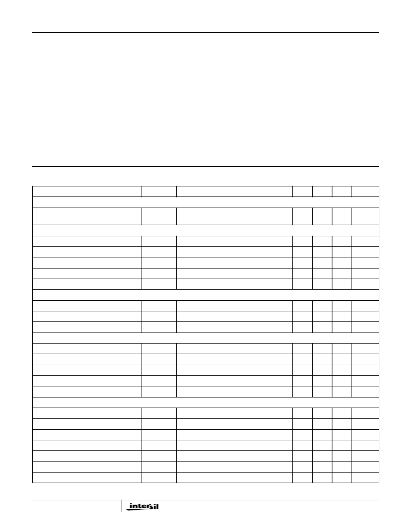
Absolute Maximum Ratings
Thermal Information
Supply Voltage, V
CC
. . . . . . . . . . . . . . . . . . . . . . . . . . . . . . . . +15V
PGOOD, RT/FAULT, DRIVE, PHASE,
and GATE Voltage . . . . . . . . . . . . . . . GND - 0.3V to V
CC
+ 0.3V
Input, Output or I/O Voltage. . . . . . . . . . . . . . . . . . GND -0.3V to 7V
ESD Classification . . . . . . . . . . . . . . . . . . . . . . . . . . . . . . . . Class 1
Operating Conditions
Supply Voltage, V
CC
. . . . . . . . . . . . . . . . . . . . . . . . . . . +12V
±
10%
Ambient Temperature Range. . . . . . . . . . . . . . . . . . . . 0
o
C to 70
o
C
Junction Temperature Range. . . . . . . . . . . . . . . . . . . 0
o
C to 125
o
C
Thermal Resistance (Typical, Note 1)
SOIC Package. . . . . . . . . . . . . . . . . . . . . . . . . . . . .
Maximum Junction Temperature (Plastic Package) . . . . . . . 150
o
C
Maximum Storage Temperature Range. . . . . . . . . . -65
o
C to 150
o
C
Maximum Lead Temperature (Soldering 10s) . . . . . . . . . . . . 300
o
C
(SOIC - Lead Tips Only)
θ
JA
(
o
C/W)
70
CAUTION: Stresses above those listed in “Absolute Maximum Ratings” may cause permanent damage to the device. This is a stress only rating and operation of the
device at these or any other conditions above those indicated in the operational sections of this specification is not implied.
NOTE:
1.
θ
JA
is measured with the component mounted on an evaluation PC board in free air.
Electrical Specifications
Recommended Operating Conditions, Unless Otherwise Noted. Refer to Block and Simplified Power System
Diagrams, and Typical Application Schematic
PARAMETER
SYMBOL
TEST CONDITIONS
MIN
TYP
MAX
UNITS
VCC SUPPLY CURRENT
Nominal Supply Current
I
CC
UGATE, LGATE, DRIVE2, DRIVE3, and
DRIVE4 Open
-
9
-
mA
POWER-ON RESET
Rising VCC Threshold
V
OCSET
= 4.5V
-
-
10.4
V
Falling VCC Threshold
V
OCSET
= 4.5V
8.2
-
-
V
Rising VAUX Threshold
V
OCSET
= 4.5V
-
2.5
-
V
VAUX Threshold Hysteresis
V
OCSET
= 4.5V
-
0.5
-
V
Rising V
OCSET
Threshold
-
1.26
-
V
OSCILLATOR
Free Running Frequency
F
OSC
RT = OPEN
185
200
215
kHz
Total Variation
6k
< RT to GND < 200k
-15
-
+15
%
Ramp Amplitude
V
OSC
RT = Open
-
1.9
-
V
P-P
DAC AND BANDGAP REFERENCE
DAC(VID0-VID4) Input Low Voltage
-
-
0.8
V
DAC(VID0-VID4) Input High Voltage
2.0
-
-
V
DACOUT Voltage Accuracy
-1.0
-
+1.0
%
Bandgap Reference Voltage
V
BG
-
1.265
-
V
Bandgap Reference Tolerance
-2.5
-
+2.5
%
LINEAR REGULATORS (OUT2, OUT3, AND OUT4)
Regulation (All Linears)
Except OUT2 when SELECT > 2.0V
-
3
-
%
VSEN2 Regulation Voltage
VREG
2
SELECT < 0.8V
-
1.5
-
V
VSEN3 Regulation Voltage
VREG
3
-
1.5
-
V
VSEN4 Regulation Voltage
VREG
4
-
1.8
-
V
Under-Voltage Level (VSEN/VREG)
VSEN
UV
VSEN Rising
-
75
-
%
Under-Voltage Hysteresis (VSEN/VREG)
VSEN Falling
-
7
-
%
Output Drive Current (All Linears)
VAUX-V
DRIVE
> 0.6V
20
40
-
mA
HIP6021A
相關(guān)PDF資料 |
PDF描述 |
|---|---|
| HIP6302CB-T | Microprocessor CORE Voltage Regulator Multi-Phase Buck PWM Controller |
| HIP6302 | Microprocessor CORE Voltage Regulator Multi-Phase Buck PWM Controller(微處理器核心多相脈寬調(diào)制解調(diào)器) |
| HIP6302CB | Microprocessor CORE Voltage Regulator Multi-Phase Buck PWM Controller |
| HIP6302VCB | Microprocessor CORE Voltage Regulator Multi-Phase Buck PWM Controller |
| HIP6302VCB-T | Microprocessor CORE Voltage Regulator Multi-Phase Buck PWM Controller |
相關(guān)代理商/技術(shù)參數(shù) |
參數(shù)描述 |
|---|---|
| HIP6028 | 制造商:INTERSIL 制造商全稱:Intersil Corporation 功能描述:Advanced PWM and Dual Linear Power Control with Integrated ACPI Support Interface |
| HIP6028CB | 制造商:Rochester Electronics LLC 功能描述:- Bulk |
| HIP6028CB WAF | 制造商:Harris Corporation 功能描述: |
| HIP6028EVAL1 | 制造商:INTERSIL 制造商全稱:Intersil Corporation 功能描述:Advanced PWM and Dual Linear Power Control with Integrated ACPI Support Interface |
| HIP6034CB | 制造商:未知廠家 制造商全稱:未知廠家 功能描述:Analog IC |
發(fā)布緊急采購,3分鐘左右您將得到回復(fù)。