- 您現(xiàn)在的位置:買賣IC網(wǎng) > PDF目錄371819 > HIN213IB (INTERSIL CORP) Hook-Up Wire; Conductor Size AWG:30; No. Strands x Strand Size:Solid; Jacket Color:Gray; Approval Bodies:UL, CSA; Approval Categories:UL AWM Style 1061; CSA AWM; Conductor Material:Copper; Jacket Material:Polyvinylchloride (PVC) RoHS Compliant: Yes PDF資料下載
參數(shù)資料
| 型號(hào): | HIN213IB |
| 廠商: | INTERSIL CORP |
| 元件分類: | 通用總線功能 |
| 英文描述: | Hook-Up Wire; Conductor Size AWG:30; No. Strands x Strand Size:Solid; Jacket Color:Gray; Approval Bodies:UL, CSA; Approval Categories:UL AWM Style 1061; CSA AWM; Conductor Material:Copper; Jacket Material:Polyvinylchloride (PVC) RoHS Compliant: Yes |
| 中文描述: | LINE TRANSCEIVER, PDSO28 |
| 封裝: | SOIC-28 |
| 文件頁(yè)數(shù): | 12/15頁(yè) |
| 文件大小: | 314K |
| 代理商: | HIN213IB |
第1頁(yè)第2頁(yè)第3頁(yè)第4頁(yè)第5頁(yè)第6頁(yè)第7頁(yè)第8頁(yè)第9頁(yè)第10頁(yè)第11頁(yè)當(dāng)前第12頁(yè)第13頁(yè)第14頁(yè)第15頁(yè)

3-12
Detailed Description
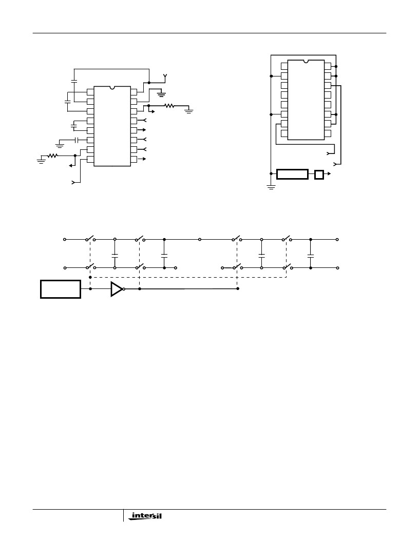
The HIN2XXE family of high-speed RS-232
transmitters/receivers are powered by a single +5V power
supply, feature low power consumption, and meet all ElA
RS232C and V.28 specifications. The circuit is divided into
three sections: the charge pump, transmitter, and receiver.
Charge Pump
An equivalent circuit of the charge pump is illustrated in
Figure 3. The charge pump contains two sections: the
voltage doubler and the voltage inverter. Each section is
driven by a two phase, internally generated clock to generate
+10V and -10V. The nominal clock frequency is 125kHz.
During phase one of the clock, capacitor C1 is charged to
V
CC
. During phase two, the voltage on C1 is added to V
CC
,
producing a signal across C3 equal to twice V
CC
. During
phase two, C2 is also charged to 2V
CC
, and then during
phase one, it is inverted with respect to ground to produce a
signal across C4 equal to -2V
CC
. The charge pump accepts
input voltages up to 5.5V. The output impedance of the
voltage doubler section (V+) is approximately 200
, and the
output impedance of the voltage inverter section (V-) is
approximately 450
. A typical application uses 0.1
μ
F
capacitors for C1-C4, however, the value is not critical.
Increasing the values of C1 and C2 will lower the output
impedance of the voltage doubler and inverter, increasing
the values of the reservoir capacitors, C3 and C4, lowers the
ripple on the V+ and V- supplies.
During shutdown mode (HIN205E, HIN206E, HIN211E,
HIN213E, HIN235E, HIN236E and HIN241E) the charge
pump is turned off, V+ is pulled down to V
CC
, V- is pulled up
to GND, and the supply current is reduced to less than 10
μ
A.
The transmitter outputs are disabled and the receiver
outputs (except for HIN213E, R4 and R5) are placed in the
high impedance state.
Transmitters
The transmitters are TTL/CMOS compatible inverters which
translate the inputs to RS-232 outputs. The input logic
threshold is about 26% of V
CC
, or 1.3V for V
CC
= 5V. A logic
Test Circuits (HIN232E)
FIGURE 1. GENERAL TEST CIRCUIT
FIGURE 2. POWER-OFF SOURCE RESISTANCE
CONFIGURATION
14
15
16
9
13
12
11
10
1
2
3
4
5
7
6
8
C1+
V+
C1-
C2+
C2-
V-
R2
IN
T2
OUT
V
CC
T1
OUT
R1
IN
R1
OUT
T1
IN
T2
IN
R2
OUT
GND
+4.5V TO
+5.5V INPUT
3k
T1 OUTPUT
RS-232
±
30V INPUT
TTL/CMOS OUTPUT
TTL/CMOS INPUT
TTL/CMOS INPUT
TTL/CMOS OUTPUT
+
-
0.1
μ
F
C3
+
-
0.1
μ
F
C1
+
-
0.1
μ
F
C2
+
-
0.1
μ
F C4
3k
OUTPUT
RS-232
±
30V INPUT
T2
14
15
16
9
13
12
11
10
1
2
3
4
5
7
6
8
C1+
V+
C1-
C2+
C2-
V-
R2
IN
T2
OUT
V
CC
T1
OUT
R1
IN
R1
OUT
T1
IN
T2
IN
R2
OUT
GND
T2
OUT
T1
OUT
V
IN
=
±
2V
A
R
OUT
= V
IN
/I
+
-
C1
+
-
C3
+
-
C2
+
-
C4
S1
S2
S5
S6
S3
S4
S7
S8
V
CC
GND
RC
OSCILLATOR
V
CC
GND
V+ = 2V
CC
GND
V
-
=
-
(V+)
C1+
C1
-
C2
-
C2+
VOLTAGE INVERTER
VOLTAGE DOUBLER
FIGURE 3. CHARGE PUMP
HIN202E thru HIN241E
相關(guān)PDF資料 |
PDF描述 |
|---|---|
| HIN202EIB | 5V High-Speed RS-232 Transceivers with 0.1uF Capacitors |
| HIN202EIB-T | 5V High-Speed RS-232 Transceivers with 0.1uF Capacitors |
| HIN202EIBN | 5V High-Speed RS-232 Transceivers with 0.1uF Capacitors |
| HIN236IB | 5V High-Speed RS-232 Transceivers with 0.1uF Capacitors |
| HIN238IB | TVS UNI 225W 27V PWRDI 123 SMD |
相關(guān)代理商/技術(shù)參數(shù) |
參數(shù)描述 |
|---|---|
| HIN213IB-T | 制造商:未知廠家 制造商全稱:未知廠家 功能描述:Interface IC |
| HIN230 | 制造商:INTERSIL 制造商全稱:Intersil Corporation 功能描述:+5V Powered RS-232 Transmitters/Receivers |
| HIN230 WAF | 制造商:Harris Corporation 功能描述: |
| HIN230CB | 制造商:Rochester Electronics LLC 功能描述:- Bulk 制造商:Harris Corporation 功能描述: |
| HIN230IB | 制造商:Rochester Electronics LLC 功能描述:- Bulk |
發(fā)布緊急采購(gòu),3分鐘左右您將得到回復(fù)。