- 您現(xiàn)在的位置:買賣IC網(wǎng) > PDF目錄383058 > HIFA1114 (Intersil Corporation) 850MHz Video Cable Driving Buffer PDF資料下載
參數(shù)資料
| 型號: | HIFA1114 |
| 廠商: | Intersil Corporation |
| 英文描述: | 850MHz Video Cable Driving Buffer |
| 中文描述: | 850MHz的視頻線驅(qū)動緩沖器 |
| 文件頁數(shù): | 2/5頁 |
| 文件大小: | 143K |
| 代理商: | HIFA1114 |
2
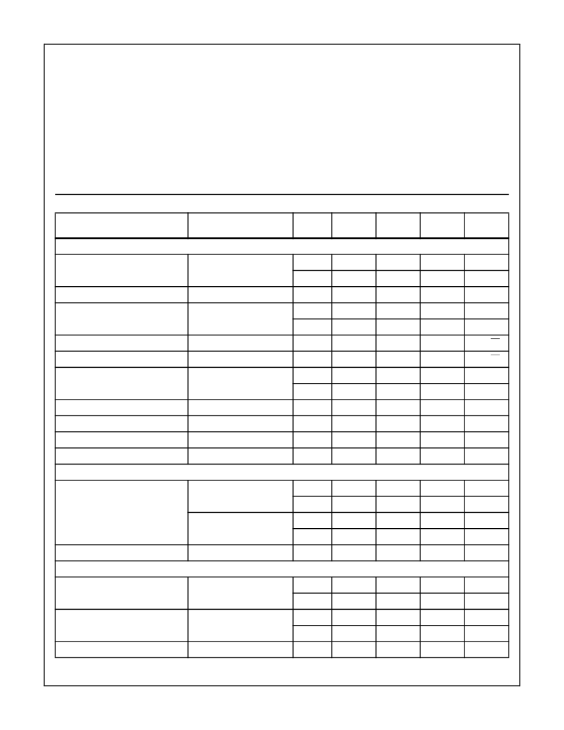
Absolute Maximum Ratings
Thermal Information
Voltage Between V+ and V- . . . . . . . . . . . . . . . . . . . . . . . . . . . . 12V
DC Input Voltage . . . . . . . . . . . . . . . . . . . . . . . . . . . . . . . V
SUPPLY
Differential Input Voltage . . . . . . . . . . . . . . . . . . . . . . . . . . . . . . . 5V
Output Current . . . . . . . . . . . . . . . . . . . . . . . . . . . . . . . . . . . . 60mA
Operating Conditions
Temperature Range . . . . . . . . . . . . . . . . . . . . . . . . . -40
o
C to 85
o
C
Thermal Resistance (Typical, Note 1)
SOIC Package. . . . . . . . . . . . . . . . . . . . . . . . . . . . .
Maximum Junction Temperature (Die) . . . . . . . . . . . . . . . . . . . 175
o
C
Maximum Junction Temperature (Plastic Package) . . . . . . . . 150
o
C
Maximum Storage Temperature Range . . . . . . . . . -65
o
C to 150
o
C
Maximum Lead Temperature (Soldering 10s). . . . . . . . . . . . 300
o
C
(SOIC - Lead Tips Only)
θ
JA
(
o
C/W)
170
CAUTION: Stresses above those listed in “Absolute Maximum Ratings” may cause permanent damage to the device. This is a stress only rating and operation
of the device at these or any other conditions above those indicated in the operational sections of this specification is not implied.
NOTE:
1.
θ
JA
is measured with the component mounted on an evaluation PC board in free air.
Electrical Specifications
V
SUPPLY
=
±
5V, A
V
= +1, R
L
= 100
,
Unless Otherwise Specified
PARAMETER
TEST
CONDITIONS
TEMP.
(
o
C)
MIN
TYP
MAX
UNITS
INPUT CHARACTERISTICS
Output Offset Voltage
25
-
8
25
mV
Full
-
-
35
mV
Output Offset Voltage Drift
Full
-
10
-
μ
V/
o
C
PSRR
25
39
45
-
dB
Full
35
-
-
dB
Input Noise Voltage
100kHz
25
-
9
-
nV/
√
Hz
Non-Inverting Input Noise Current
100kHz
25
-
37
-
pA/
√
Hz
Non-Inverting Input Bias Current
25
-
25
40
μ
A
Full
-
-
65
μ
A
Non-Inverting Input Resistance
25
25
50
-
k
Inverting Input Resistance
25
240
300
360
Input Capacitance
Either Input
25
-
2
-
pF
Input Common Mode Range
Full
±
2.5
±
2.8
-
V
TRANSFER CHARACTERISTICS
Gain
A
V
= +1, V
IN
= +2V
25
0.980
0.990
1.02
V/V
Full
0.975
-
1.025
V/V
A
V
= +2, V
IN
= +1V
25
1.96
1.98
2.04
V/V
Full
1.95
-
2.05
V/V
DC Non-Linearity
A
V
= +2,
±
2V Full Scale
25
-
0.02
-
%
OUTPUT CHARACTERISTICS
Output Voltage
A
V
= -1
25
±
3.0
±
3.3
-
V
Full
±
2.5
±
3.0
-
V
Output Current
A
V
= -1, R
L
= 50
25, 85
50
60
-
mA
-40
o
C
35
50
-
mA
Closed Loop Output Impedance
A
V
= +2, DC
25
-
0.3
-
HFA1114
相關(guān)PDF資料 |
PDF描述 |
|---|---|
| HIP1012CB-T | Dual Power Distribution Controller |
| HIP1012ACB | Dual Power Distribution Controller |
| HIP1012CB | 512 MACROCELL 3.3 VOLT ZERO POWER ISP CP - NOT RECOMMENDED for NEW DESIGN |
| HIP1012ACB-T | Dual Power Distribution Controller |
| HIP1030AS | 1A High Side Driver with Overload Protection |
相關(guān)代理商/技術(shù)參數(shù) |
參數(shù)描述 |
|---|---|
| HIF-B | 功能描述:熔絲座 BUSS FUSEHOLDER RoHS:否 制造商:Littelfuse 產(chǎn)品: 電流額定值:30 A 電壓額定值:1000 VDC 極數(shù):1 系列: 安裝風(fēng)格:DIN Rail 端接類型: 軸類型: 工作溫度范圍: |
| HIFB-26D-1.27R | 制造商:Hirose 功能描述: |
| HIFD1L | 制造商:Hubbell Wiring Device-Kellems 功能描述:HOUSING, DEVICE BOX,CAST ALUM,1/2 |
| HIFD2L | 制造商:Hubbell Wiring Device-Kellems 功能描述:HOUSING, DEVICE BOX,CAST ALUM,3/4 |
| HIFH-80PA-1.27DSA | 制造商:Hirose 功能描述: |
發(fā)布緊急采購,3分鐘左右您將得到回復(fù)。