- 您現(xiàn)在的位置:買賣IC網(wǎng) > PDF目錄371812 > HI1176JCQ (INTERSIL CORP) Small glass bead with axial leads PDF資料下載
參數(shù)資料
| 型號: | HI1176JCQ |
| 廠商: | INTERSIL CORP |
| 元件分類: | ADC |
| 英文描述: | Small glass bead with axial leads |
| 中文描述: | 1-CH 8-BIT FLASH METHOD ADC, PARALLEL ACCESS, PQFP32 |
| 封裝: | 7 X 7 MM, ROHS COMPLIANT, MQFP-32 |
| 文件頁數(shù): | 3/11頁 |
| 文件大小: | 85K |
| 代理商: | HI1176JCQ |
4-3
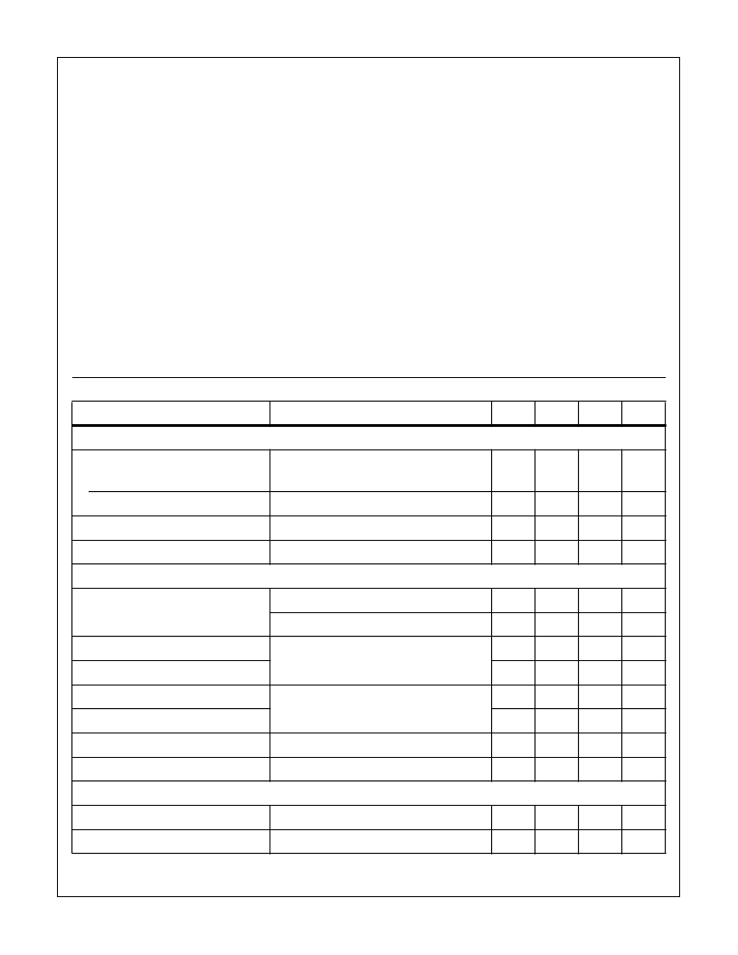
Absolute Maximum Ratings
Thermal Information
Supply Voltage, V
DD
. . . . . . . . . . . . . . . . . . . . . . . . . . . . . . . . . . . 7V
Reference Voltage, V
RT
, V
RB
. . . . . . . . . V
DD
+ 0.5V to V
SS
- 0.5V
Analog Input Voltage, V
IN
. . . . . . . . . . . . . V
DD
+ 0.5V to V
SS
- 0.5V
Digital Input Voltage, CLK. . . . . . . . . . . . . V
DD
+ 0.5V to V
SS
- 0.5V
Digital Output Voltage, V
OH
, V
OL
. . . . . . . V
DD
+ 0.5V to V
SS
- 0.5V
Operating Conditions
(Note 1)
Temperature Range, T
A
. . . . . . . . . . . . . . . . . . . . . . . -40
o
C to 85
o
C
Supply Voltage
AV
DD
, AV
SS
, DV
DD
, DV
SS
. . . . . . . . . . . . . . . +4.75V to +5.25V
|DGND-AGND| . . . . . . . . . . . . . . . . . . . . . . . . . . . .0mV to 100mV
Reference Input Voltage
V
RB
. . . . . . . . . . . . . . . . . . . . . . . . . . . . . . . . . . . . . 0V and Above
V
RT
. . . . . . . . . . . . . . . . . . . . . . . . . . . . . . . . . . . . 2.8V and Below
Analog Input Voltage, V
IN
. . . . . . . . . V
RB
to V
RT
(1.8V
P-P
to AV
DD
)
Clock Pulse Width
t
PW1
. . . . . . . . . . . . . . . . . . . . . . . . . . . . . . . . . . . . . . . 25ns (Min)
t
PW0
. . . . . . . . . . . . . . . . . . . . . . . . . . . . . . . . . . . . . . . 25ns (Min)
CAUTION: Stresses above those listed in “Absolute Maximum Ratings” may cause permanent damage to the device. This is a stress only rating and operation of
the device at these or any other conditions above those indicated in the operational sections of this specification is not implied.
Thermal Resistance (Typical, Note 1)
MQFP Package . . . . . . . . . . . . . . . . . . . . . . . . . . . .
Maximum Junction Temperature . . . . . . . . . . . . . . . . . . . . . . . 150
o
C
Maximum Storage Temperature Range . . . . . . . . . -65
o
C to 150
o
C
Maximum Lead Temperature (Soldering 10s). . . . . . . . . . . . . 300
o
C
(Lead Tips Only)
θ
JA
(
o
C/W)
122
NOTE:
1.
θ
JA
is measured with the component mounted on an evaluation PC board in free air.
Electrical Specifications
f
C
= 20 MSPS, V
DD
= +5V, V
RB
= 0.5V, V
RT
= 2.5V, T
A
= 25
o
C (Note 1)
PARAMETER
TEST CONDITIONS
MIN
TYP
MAX
UNIT
SYSTEM PERFORMANCE
Offset Voltage
E
OT
-60
-40
-20
mV
E
OB
+20
+40
+60
mV
Integral Non-Linearity, INL
f
C
= 20 MSPS, V
IN
= 0.5V to 2.5V
-
±
0.5
±
1.3
LSB
Differential Non-Linearity, DNL
f
C
= 20 MSPS, V
IN
= 0.5V to 2.5V
-
±
0.3
±
0.5
LSB
DYNAMIC CHARACTERISTICS
Signal to Noise Ratio, SINAD
f
S
= 20MHz, f
IN
= 1MHz
-
46
-
dB
f
S
= 20MHz, f
IN
= 3.58MHz
-
46
-
dB
Maximum Conversion Speed, f
C
V
IN
= 0.5V to 2.5V, f
IN
= 1kHz Ramp
20
35
-
MSPS
Minimum Conversion Speed
-
-
0.5
MSPS
Differential Gain Error, DG
NTSC 40 IRE Mod Ramp, f
C
= 14.3 MSPS
-
1.0
-
%
Differential Phase Error, DP
-
0.5
-
Degree
Aperture Jitter, t
AJ
-
30
-
ps
Sampling Delay, t
DS
-
4
-
ns
ANALOG INPUTS
Analog Input Bandwidth (-1dB), BW
-
18
-
MHz
Analog Input Capacitance, C
IN
V
IN
= 1.5V + 0.07V
RMS
-
11
-
pF
----------------------------------------------------------------------------------------------------------------
HI1176
相關(guān)PDF資料 |
PDF描述 |
|---|---|
| HI1176-EV | 8-Bit, 20 MSPS, Flash A/D Converter |
| HI1176 | 8-Bit, 20 MSPS, Flash A/D Converter |
| HI1177JCQ | 8-Bit, 40MSPS, 2-Channel D/A Converter |
| HI1177 | 8-Bit, 40MSPS, 2-Channel D/A Converter |
| HI1178JCQ | Triple 8-Bit, 40 MSPS, RGB, 3-Channel D/A Converter |
相關(guān)代理商/技術(shù)參數(shù) |
參數(shù)描述 |
|---|---|
| HI1176JCQ-T | 制造商:Rochester Electronics LLC 功能描述:- Bulk |
| HI1177 | 制造商:INTERSIL 制造商全稱:Intersil Corporation 功能描述:8-Bit, 40MSPS, 2-Channel D/A Converter |
| HI1177JCQ | 制造商:Rochester Electronics LLC 功能描述:32 PQFP INDTEMP DUAL VIDEO D/A 8BIT 40MHZ - Bulk 制造商:Harris Corporation 功能描述: |
| HI1177JCQ-T | 制造商:Rochester Electronics LLC 功能描述:HI1177JCQ IN TAPE & REEL - Tape and Reel 制造商:Harris Corporation 功能描述: |
| HI1178 | 制造商:INTERSIL 制造商全稱:Intersil Corporation 功能描述:Triple 8-Bit, 40 MSPS, RGB, 3-Channel D/A Converter |
發(fā)布緊急采購,3分鐘左右您將得到回復(fù)。