- 您現(xiàn)在的位置:買賣IC網(wǎng) > PDF目錄370500 > HDSP-253X Eight Character 5 mm Smart Alphanumeric Display PDF資料下載
參數(shù)資料
| 型號: | HDSP-253X |
| 英文描述: | Eight Character 5 mm Smart Alphanumeric Display |
| 中文描述: | 八字5毫米智能字符顯示 |
| 文件頁數(shù): | 12/16頁 |
| 文件大小: | 417K |
| 代理商: | HDSP-253X |

12
Self Test Function (Bits 5, 6)
Bit 6 of the Control Word Regis-
ter is used to initiate the self test
function. Results of the internal
self test are stored in bit 5 of the
Control Word. Bit 5 is a read only
bit where bit 5 = “1” indicates a
passed self test and bit 5 = “0”
indicates a failed self test.
Setting bit 6 to a logic 1 will start
the self test function. The built-in
self test function of the IC
consists of two internal routines
which exercises major portions of
the IC and illuminates all of the
LEDs. The first routine cycles the
ASCII decoder ROM through all
states and performs a checksum
on the output. If the checksum
agrees with the correct value, bit
5 is set to “1.” The second routine
provides a visual test of the LEDs
using the drive circuitry. This is
accomplished by writing
checkered and inverse checkered
patterns to the display. Each
pattern is displayed for approxi-
mately 2 seconds.
During the self test function the
display must not be accessed. The
time needed to execute the self
test function is calculated by
multiplying the clock period by
262,144. For example, assume a
clock frequency of 58 KHz, then
the time to execute the self test
function frequency is equal to
(262,144/58,000) = 4.5 second
duration.
At the end of the self test func-
tion, the Character RAM is loaded
with blanks, the Control Word
Register is set to zeros except for
bit 5, and the Flash RAM is
cleared and the UDC Address
Register is set to all ones.
Clear Function (Bit 7)
Bit 7 of the Control Word will
clear the Character RAM and the
Flash RAM. Setting bit 7 to a “1”
will start the clear function. Three
clock cycles (110
μ
s min. using
the internal refresh clock) are
required to complete the clear
function. The display must not be
accessed while the display is
being cleared. When the clear
function has been completed, bit
7 will be reset to a “0.” The ASCII
character code for a space (20H)
will be loaded into the Character
RAM to blank the display and the
Flash RAM will be loaded with
“1”s. The UDC RAM, UDC
Address Register and the re-
mainder of the Control Word are
unaffected.
Display Reset
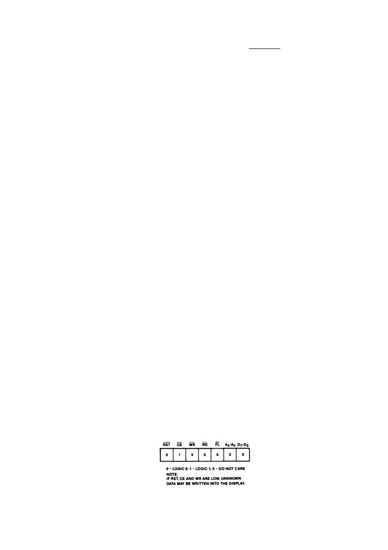
Figure 7 shows the logic levels
needed to reset the display. The
display should be reset on Power-
up. The external Reset clears the
Character RAM, Flash RAM,
Control Word and resets the
internal counters. After the rising
edge of the Reset signal, three
clock cycles (110
μ
s min. using
the internal refresh clock) are
required to complete the reset
sequence. The display must not
be accessed while the display is
being reset. The ASCII Character
code for a space (20H) will be
loaded into the Character RAM to
blank the display. The Flash RAM
and Control Word Register are
loaded with all "0"s. The UDC
RAM and UDC Address Register
are unaffected. All displays which
operate with the same clock
source must be simultaneously
reset to synchronize the Flashing
and Blinking functions.
Mechanical
Considerations
The HDSP-253X is assembled by
die attaching and wire bonding
280 LED chips and a CMOS IC to
a thermally conductive printed
circuit board. A polycarbonate
lens placed over the pcb creates
an air gap over the LED wire
bonds. A backfill epoxy seals the
display package.
Figure 8 shows the proper
method to insert the display by
hand. To prevent damage to the
LED wire bonds, apply pressure
uniformly with fingers located at
both ends of the part. Using a
tool, shown in Figure 9, such as a
screwdriver or pliers to push the
display into the printed circuit
board or socket may damage the
LED wire bonds. The force
exerted by a screwdriver is
sufficient to push the lens into the
LED wire bonds. The bent wire
bonds cause shorts or opens that
result in catastrophic failure of
the LEDs.
Figure 7. Logic Levels to Reset the Display.
相關(guān)PDF資料 |
PDF描述 |
|---|---|
| HDSP-303Y | 10 mm 1 Digit Slim Font Display(10 mm 1位數(shù)字細(xì)字型前端顯示器) |
| HDSP-301G | 10 mm 1 Digit Slim Font Display(10 mm 1位數(shù)字細(xì)字型前端顯示器) |
| HDSP-301Y | 10 mm 1 Digit Slim Font Display(10 mm 1位數(shù)字細(xì)字型前端顯示器) |
| HDSP-303A | 10 mm 1 Digit Slim Font Display(10 mm 1位數(shù)字細(xì)字型前端顯示器) |
| HDSP-303G | 10 mm 1 Digit Slim Font Display(10 mm 1位數(shù)字細(xì)字型前端顯示器) |
相關(guān)代理商/技術(shù)參數(shù) |
參數(shù)描述 |
|---|---|
| HDSP-301A | 功能描述:LED 顯示器和配件 Red 643nm 10mm 7 Segment RoHS:否 制造商:Avago Technologies 顯示器類型:7 Segment 數(shù)位數(shù)量:2 字符大小:7.8 mm x 14.22 mm 照明顏色:Red 波長:628 nm 共用管腳:Common Anode 工作電壓:2.05 V 工作電流:20 mA 最大工作溫度:+ 85 C 最小工作溫度:- 35 C 封裝:Tube |
| HDSP-301E | 功能描述:LED 顯示器和配件 Red 625nm 10mm 7 Segment RoHS:否 制造商:Avago Technologies 顯示器類型:7 Segment 數(shù)位數(shù)量:2 字符大小:7.8 mm x 14.22 mm 照明顏色:Red 波長:628 nm 共用管腳:Common Anode 工作電壓:2.05 V 工作電流:20 mA 最大工作溫度:+ 85 C 最小工作溫度:- 35 C 封裝:Tube |
| HDSP-301G | 功能描述:LED 顯示器和配件 Green 573nm 10mm 7 Segment RoHS:否 制造商:Avago Technologies 顯示器類型:7 Segment 數(shù)位數(shù)量:2 字符大小:7.8 mm x 14.22 mm 照明顏色:Red 波長:628 nm 共用管腳:Common Anode 工作電壓:2.05 V 工作電流:20 mA 最大工作溫度:+ 85 C 最小工作溫度:- 35 C 封裝:Tube |
| HDSP-301Y | 功能描述:LED 顯示器和配件 Yellow 590nm 10mm 7 Segment RoHS:否 制造商:Avago Technologies 顯示器類型:7 Segment 數(shù)位數(shù)量:2 字符大小:7.8 mm x 14.22 mm 照明顏色:Red 波長:628 nm 共用管腳:Common Anode 工作電壓:2.05 V 工作電流:20 mA 最大工作溫度:+ 85 C 最小工作溫度:- 35 C 封裝:Tube |
| HDSP-303A | 功能描述:LED 顯示器和配件 Red 643nm 10mm 7 Segment RoHS:否 制造商:Avago Technologies 顯示器類型:7 Segment 數(shù)位數(shù)量:2 字符大小:7.8 mm x 14.22 mm 照明顏色:Red 波長:628 nm 共用管腳:Common Anode 工作電壓:2.05 V 工作電流:20 mA 最大工作溫度:+ 85 C 最小工作溫度:- 35 C 封裝:Tube |
發(fā)布緊急采購,3分鐘左右您將得到回復(fù)。