- 您現(xiàn)在的位置:買賣IC網(wǎng) > PDF目錄223876 > HCPL-J312 2.0 Amp Output Current IGBT Gate Drive Optocoupler PDF資料下載
參數(shù)資料
| 型號(hào): | HCPL-J312 |
| 英文描述: | 2.0 Amp Output Current IGBT Gate Drive Optocoupler |
| 中文描述: | 2.0安培輸出電流IGBT柵極驅(qū)動(dòng)光電耦合器 |
| 文件頁數(shù): | 9/12頁 |
| 文件大小: | 264K |
| 代理商: | HCPL-J312 |
6
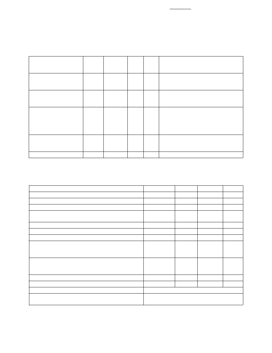
Absolute Maximum Ratings (No Derating Required up to 85
°C)
Parameter
Symbol
Min.
Max.
Units
Storage Temperature
TS
-55
125
°C
Operating Temperature
TA
-40
85
°C
Average Forward Input Current
IF(AVG)
20
mA
Peak Forward Input Current
IFPK
40
mA
(50% Duty Cycle, 1 ms Pulse Width)
Reverse Input Voltage (Each Channel)
VR
5V
Input Power Dissipation (Each Channel)
PI
35
mW
Output Current (Each Channel)
IO
60
mA
Supply Voltage and Output Voltage
VCC
-0.5
18
V
(HCPL-2731, HCPL-0731)
(VCC - Pin 8-5, VO - Pin 7,6-5) -Note 1
Supply Voltage and Output Voltage
VCC
-0.5
7
V
(HCPL-2730, HCPL-0730)
(VCC - Pin 8-5, VO - Pin 7,6-5) -Note 1
Output Power Dissipation (Each Channel) -Note 12
PO
100
mW
Total Power Dissipation (Each Channel)
PT
135
mW
Lead Solder Temperature (for Through Hole Devices)
260
°C for 10 sec., 1.6 mm below seating plane
Reflow Temperature Profile
See Package Outline Drawings section
(for SOIC-8 and Option #300)
Insulation Related Specifications (HCPL-2731/2730/0731/0730)
8-Pin DIP
(300 Mil)
SO-8
Parameter
Symbol
Value
Units
Conditions
Minimum External Air
L(101)
7.1
4.9
mm
Measured from input terminals to
Gap (External
output terminals, shortest distance
Clearance)
through air.
Minimum External
L(102)
7.4
4.8
mm
Measured from input terminals to
Tracking (External
output terminals, shortest distance
Creepage)
path along body.
Minimum Internal Plastic
0.08
mm
Through insulation distance, conductor
Gap (Internal Clearance)
to conductor, usually the direct
distance between the photoemitter and
photodetector inside the optocoupler
cavity.
Tracking Resistance
CTI
200
Volts
DIN IEC 112/ VDE 0303 Part 1
(Comparative Tracking
Index)
Isolation Group
IIIa
Material Group DIN VDE 0110
Option 300 – surface mount classification is Class A in accordance with CECC 00802.
相關(guān)PDF資料 |
PDF描述 |
|---|---|
| HCPL-J456 | SCHMITT-TRIGGER-OUTPUT OPTOCOUPLER |
| HCPL-J784-300 | Receptacle With A Standard Tail |
| HCPL-T250 | FET-OUTPUT OPTOCOUPLER |
| HCPL-3100-300 | 1 CHANNEL LOGIC OUTPUT OPTOCOUPLER |
| HCPL-4504#300E | 1 CHANNEL LOGIC OUTPUT OPTOCOUPLER |
相關(guān)代理商/技術(shù)參數(shù) |
參數(shù)描述 |
|---|---|
| HCPL-J312#300 | 功能描述:邏輯輸出光電耦合器 2.0A IGBT Gate Drive RoHS:否 制造商:Fairchild Semiconductor 絕緣電壓:4243 Vrms 輸出類型:Push-Pull 最大傳播延遲時(shí)間:500 ns 最大正向二極管電壓: 最大反向二極管電壓: 最大正向二極管電流: 最大連續(xù)輸出電流:2.5 A 最大功率耗散:100 mW 最大工作溫度:+ 100 C 最小工作溫度:- 40 C 封裝 / 箱體:SO-16 封裝:Tube |
| HCPL-J312#500 | 功能描述:邏輯輸出光電耦合器 2.0A IGBT Gate Drive RoHS:否 制造商:Fairchild Semiconductor 絕緣電壓:4243 Vrms 輸出類型:Push-Pull 最大傳播延遲時(shí)間:500 ns 最大正向二極管電壓: 最大反向二極管電壓: 最大正向二極管電流: 最大連續(xù)輸出電流:2.5 A 最大功率耗散:100 mW 最大工作溫度:+ 100 C 最小工作溫度:- 40 C 封裝 / 箱體:SO-16 封裝:Tube |
| HCPL-J312-000E | 功能描述:邏輯輸出光電耦合器 2.0A IGBT Gate Drive RoHS:否 制造商:Fairchild Semiconductor 絕緣電壓:4243 Vrms 輸出類型:Push-Pull 最大傳播延遲時(shí)間:500 ns 最大正向二極管電壓: 最大反向二極管電壓: 最大正向二極管電流: 最大連續(xù)輸出電流:2.5 A 最大功率耗散:100 mW 最大工作溫度:+ 100 C 最小工作溫度:- 40 C 封裝 / 箱體:SO-16 封裝:Tube |
| HCPL-J312-300E | 功能描述:邏輯輸出光電耦合器 2.0A IGBT Gate Drive RoHS:否 制造商:Fairchild Semiconductor 絕緣電壓:4243 Vrms 輸出類型:Push-Pull 最大傳播延遲時(shí)間:500 ns 最大正向二極管電壓: 最大反向二極管電壓: 最大正向二極管電流: 最大連續(xù)輸出電流:2.5 A 最大功率耗散:100 mW 最大工作溫度:+ 100 C 最小工作溫度:- 40 C 封裝 / 箱體:SO-16 封裝:Tube |
| HCPL-J312-500E | 功能描述:邏輯輸出光電耦合器 2.0A IGBT Gate Drive RoHS:否 制造商:Fairchild Semiconductor 絕緣電壓:4243 Vrms 輸出類型:Push-Pull 最大傳播延遲時(shí)間:500 ns 最大正向二極管電壓: 最大反向二極管電壓: 最大正向二極管電流: 最大連續(xù)輸出電流:2.5 A 最大功率耗散:100 mW 最大工作溫度:+ 100 C 最小工作溫度:- 40 C 封裝 / 箱體:SO-16 封裝:Tube |
發(fā)布緊急采購,3分鐘左右您將得到回復(fù)。