- 您現(xiàn)在的位置:買賣IC網(wǎng) > PDF目錄370396 > GT4122-CKF Analog Multiplier PDF資料下載
參數(shù)資料
| 型號(hào): | GT4122-CKF |
| 英文描述: | Analog Multiplier |
| 中文描述: | 模擬乘法器 |
| 文件頁(yè)數(shù): | 10/15頁(yè) |
| 文件大小: | 387K |
| 代理商: | GT4122-CKF |
第1頁(yè)第2頁(yè)第3頁(yè)第4頁(yè)第5頁(yè)第6頁(yè)第7頁(yè)第8頁(yè)第9頁(yè)當(dāng)前第10頁(yè)第11頁(yè)第12頁(yè)第13頁(yè)第14頁(yè)第15頁(yè)

520 - 44 - 00
NON - VIDEO APPLICATIONS
The previous applications use the GT4122 as an overall unity
gain, non-inverting system. With this same configuration it is
possible to make a simple Amplitude Modulator. It is also
possible to configure either input stage as an inverting amplifier
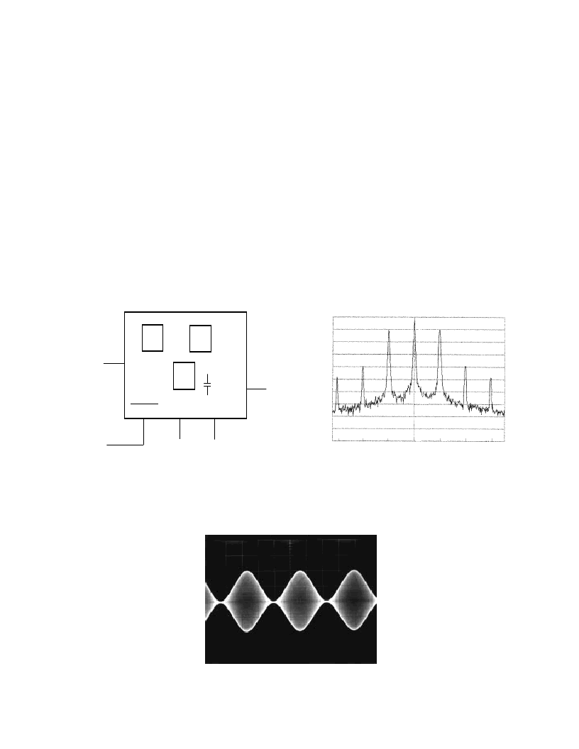
Photograph 9. Envelope Waveform of A.M. Signal
An Amplitude Modulator circuit is shown in Figure 8 and
produces an output spectrum as shown in Figure 9. The
resulting envelope waveform is shown in Photograph 9. For
this application, a 1V peak to peak, 1 MHz carrier is applied to
the non-inverting B-INPUT.
A 3kHz, 1V peak to peak audio signal is applied to the
CONTROL input superimposed on a +0.5V DC bias. The bias
centres the CONTROL signal with respect to the 0.5V DC
REFERENCE voltage.
Modulation is achieved by varying the CONTROL signal at the
audio rate which in turn allows more or less of the carrier,
appearing on B-INPUT, through to the OUTPUT.
Post mixing of this signal would place the carrier on any
desired RF channel.
0
-20
-40
-60
-80
-100 -9k -6k -3k 1M 3k 6k 9k
FREQUENCY (Hz)
Fig. 9 Spectrum of A.M. Signal
RV1
1V P-P TRIANGLE
WAVE AT15 kHz
(V = 0 to 1V)
DC OFFSET = 0.5V
CONTROL
INPUT
A - IN
B - IN
STROBE
OUT
O/C
GND
1.0V
RV2
RV3
TO
SCOPE
CHOLD
Fig. 8 Amplitude Modulator Circuit
and produce anti-phase signals which are then applied to the
internal summing circuits. This allows the device to be used
as a Double Sideband Balanced Modulator. Both of these
applications are described below.
AMPLITUDE MODULATOR
G
相關(guān)PDF資料 |
PDF描述 |
|---|---|
| GT4123ACDA | Analog Multiplier |
| GT4123ACKA | Analog Multiplier |
| GT4123-CDA | Analog Multiplier |
| GT4123-CKA | Analog Multiplier |
| GT4124 | Trimmable Two Input Analog Mixers |
相關(guān)代理商/技術(shù)參數(shù) |
參數(shù)描述 |
|---|---|
| GT4123 | 制造商:GENNUM 制造商全稱:GENNUM 功能描述:Two Channel Video Multipliers |
| GT4123/A | 制造商:未知廠家 制造商全稱:未知廠家 功能描述:Trimless Two Input Analog Mixers |
| GT4123A | 制造商:GENNUM 制造商全稱:GENNUM 功能描述:Two Channel Video Multipliers |
| GT4123ACDA | 制造商:Rochester Electronics LLC 功能描述: 制造商:Gennum Corporation 功能描述: |
| GT4123ACKA | 制造商:Rochester Electronics LLC 功能描述: 制造商:Gennum Corporation 功能描述: |
發(fā)布緊急采購(gòu),3分鐘左右您將得到回復(fù)。