- 您現(xiàn)在的位置:買賣IC網(wǎng) > PDF目錄64980 > GM393 (American Power Management Inc.) LOW POWER DUAL DIFFERENTIAL COMPARATOR PDF資料下載
參數(shù)資料
| 型號(hào): | GM393 |
| 廠商: | American Power Management Inc. |
| 英文描述: | LOW POWER DUAL DIFFERENTIAL COMPARATOR |
| 中文描述: | 低功耗雙差分比較器 |
| 文件頁(yè)數(shù): | 4/8頁(yè) |
| 文件大?。?/td> | 141K |
| 代理商: | GM393 |
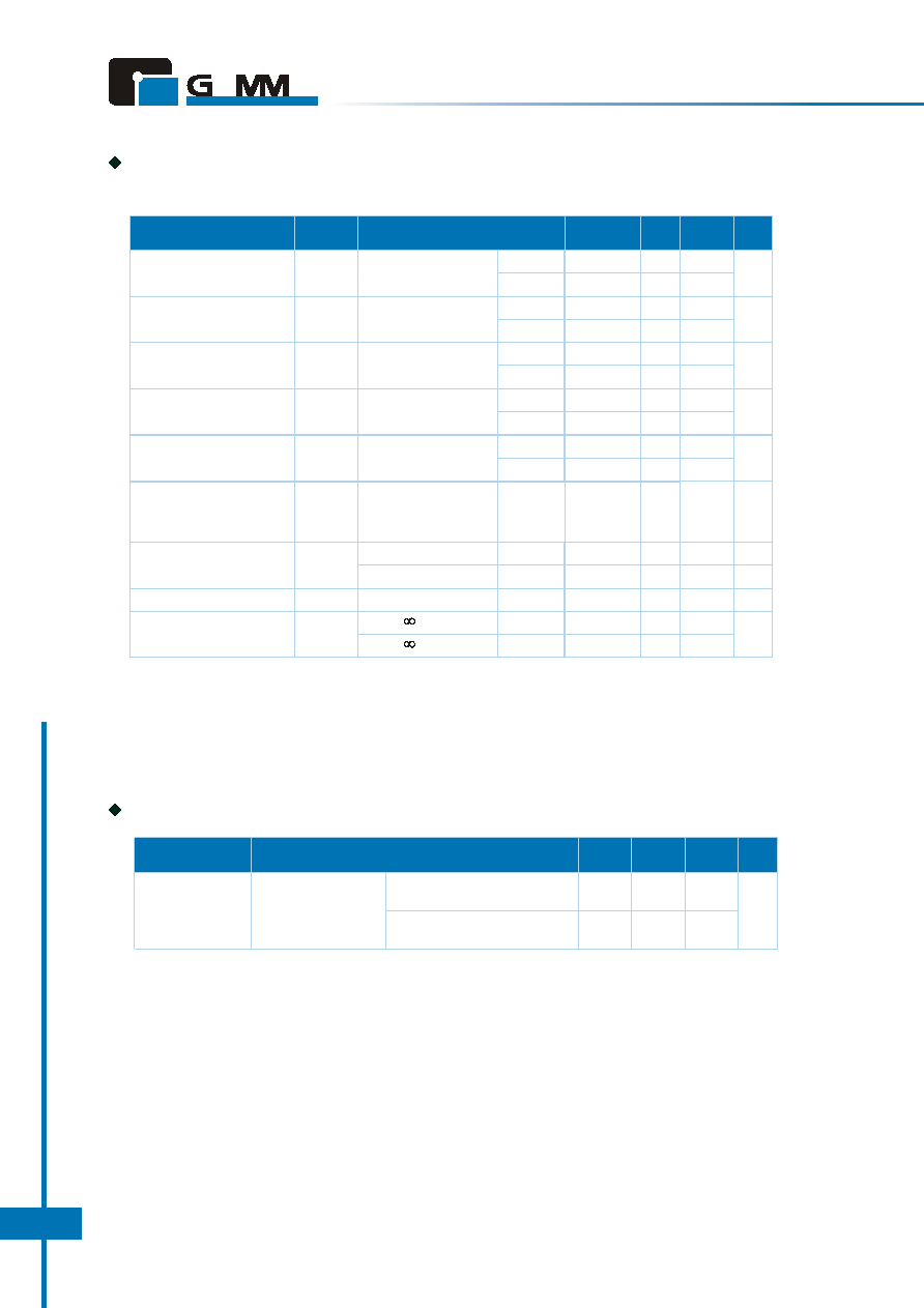
ELECTRICAL CHARACTERISTICS
(V
= 5V, at specified free - air temperature, unless otherwise specified)
CC
G
M
3
9
3
4
TEST CONDITIONS
MIN
TYP
MAX
UNIT
CHARACTERISTICS
Input Offset Voltage
Input Offset Current
Input Bias Current
Common - Mode Input Voltage
Range **
Low - Level Output Voltage
Large - Signal Differential
Voltage Amplification
V
= 1.4V
O
±2
±5
-25
mV
nA
±5
±50
9
±150
-250
400
SYMBOL
VIO
IIO
IIB
VICR
VOL
AVD
V
= 5V to 30V,
CC
V
= V
min, V = 1.4V
CC
ICR
O
25°C
Full range
25°C
Full range
V
= 1.4V
O
0 to V
- 1.5
CC
V
0 to V
- 2
CC
I
= 4mA, V
= -1V
OL
ID
V
= 15V, V = 14V
CC
O
to 11.4V,
R > 15kW to V
LCC
150
50
400
200
700
mV
V/ mV
High - Level Output Curretn
Low - Level Output Current
IOH
IOL
25°C
Full range
V
= 5V, V
= 1V
OH
ID
V
= 1.5V, V
= -1V
OL
ID
0.1
50
1
nA
mA
V
= 30V, V
= 1V
OH
ID
A
6
Supply Current
ICC
25°C
Full range
R =
, V
= 5V
LCC
0.8
1.0
2.5
R =
, V
= 30V
LCC
mA
* All characteristics are measured under open loop conditions with zero common - mode input voltage unless otherwise
specified. Full range is 0°C to 70°C.
** The voltage at either input or common - mode should not be allowed to go negative by more than 0.3V.
The upper end of the common - mode voltage range is V
- 1.5V, but either or both inputs can go to 30V without damage.
CC
nA
SWITCHING CHARACTERISTICS, V
= 5V, TA=25°C
CC
TEST CONDITIONS
MIN
TYP
MAX
UNIT
PARAMETER
Response time
R Connected to 5V
L
through 5.1kW,
C = 15pF* (See Note 1)
L
100 - mV input step with 5 - mV
overdrive
TTL - level input step
1.3
0.3
s
* C includes probe and jig capacitance.
L
Note 1: The response time specified is the interval between the input step function and the instant when the output
crosses 1.4V.
A
MICROELECTRONICS
GM393
LOW POWER DUAL DIFFERENTIAL COMPARATOR
Signal Conditioning
相關(guān)PDF資料 |
PDF描述 |
|---|---|
| gm393 | Op-Amp Comparators |
| GM431A | Adjustable Shunt Regulators |
| gm431b | Adjustable Shunt Regulators |
| GM6155-2.5ST25R | 150mA LOW-NOISE LDO REGULATOR |
| GM6155-2.7ST25R | 150mA LOW-NOISE LDO REGULATOR |
相關(guān)代理商/技術(shù)參數(shù) |
參數(shù)描述 |
|---|---|
| GM393_1 | 制造商:GAMMA 制造商全稱:GAMMA 功能描述:LOW POWER DUAL DIFFERENTIAL COMPARATOR |
| GM393D8T | 制造商:GAMMA 制造商全稱:GAMMA 功能描述:LOW POWER DUAL DIFFERENTIAL COMPARATOR |
| GM393S8R | 制造商:GAMMA 制造商全稱:GAMMA 功能描述:LOW POWER DUAL DIFFERENTIAL COMPARATOR |
| GM393S8T | 制造商:GAMMA 制造商全稱:GAMMA 功能描述:LOW POWER DUAL DIFFERENTIAL COMPARATOR |
| GM39COG4R7C050AD | 制造商:MURATA 功能描述:0603X004R7 MURATA NXE5A |
發(fā)布緊急采購(gòu),3分鐘左右您將得到回復(fù)。