- 您現(xiàn)在的位置:買賣IC網(wǎng) > PDF目錄382994 > G920 (Electronic Theatre Controls, Inc.) 150mA Micro-power LDO Regulators PDF資料下載
參數(shù)資料
| 型號: | G920 |
| 廠商: | Electronic Theatre Controls, Inc. |
| 元件分類: | 基準(zhǔn)電壓源/電流源 |
| 英文描述: | 150mA Micro-power LDO Regulators |
| 中文描述: | 150mA的微功率LDO穩(wěn)壓器 |
| 文件頁數(shù): | 5/7頁 |
| 文件大小: | 122K |
| 代理商: | G920 |
Ver 0.0 Preliminary
Mar 27, 2001
TEL: 886-3-5788833
http://www.gmt.com.tw
5
G920
Global Mixed-mode Technology Inc.
Pin Description
PIN
1
2
NAME
NC
IN
FUNCTION
This is a NC pin, should be left unconnected.
Regulator Input. Supply voltage can range from +2.5V to +6.5V. Bypass with 1μF to GND.
Regulator Output. Sources up to 150mA. Bypass with a 1μF,
<
0.2
typical ESR capacitor to
GND.
Active-High Enable Input. A logic low reduces the supply current to less than 1
μ
A. Connect to IN for
normal operation.
Ground. This pin also functions as a heatsink. Solder to large pads or the circuit board ground
plane to maximize thermal dissipation.
3
OUT
4
EN
5,6,7,8
GND
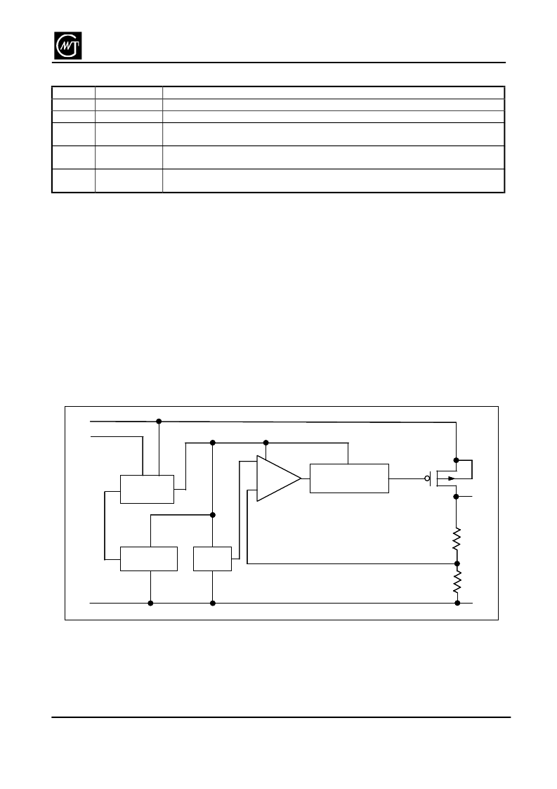
Detailed Description
The block diagram of the G920 is shown in Figure 1. It
consists of an error amplifier, 1.25V bandgap refer-
ence, PMOS output transistor, internal feedback
voltage divider, shutdown logic, over current protection
circuit, and over temperature protection circuit.
The internal feedback voltage divider’s central tap is
connected to the non-inverting input of the error ampli-
fier. The error amplifier compares non-inverting input
with the 1.25V bandgap reference. If the feedback
voltage is higher than 1.25V, the error amplifier’s out-
put becomes higher so that the PMOS output transis-
tor has a smaller gate-to-source voltage (V
GS
). This
reduces the current carrying capability of the PMOS
output transistor, as a result the output voltage de-
creases until the feedback v41oltage is equal to 1.25V.
Similarly, when the feedback voltage is less than
1.25V, the error amplifier causes the output PMOS to
conductor more current to pull the feedback voltage up
to 1.25V. Thus, through this feedback action, the error
amplifier, output PMOS, and the voltage divider effec-
tively form a unity-gain amplifier with the feedback
voltage force to be the same as the 1.25V bandgap
reference. The output voltage, V
OUT
, is then given by
the following equation:
V
OUT
= 1.25 (1 + R1/R2).
(1)
For the G920, the pre-set output voltage is 3.3V.
Figure 1. Functional Diagram
EN
IN
OUT
LOGIC
Vref
-
+
FEEDBACK
GND
R1
R2
PROTECT
SHUTDOWN
1.25V
ERROR
AMP
OVER CURRENT
PROTECT & DYNAMIC
OVER TEMP.
相關(guān)PDF資料 |
PDF描述 |
|---|---|
| G93-016-210-AGGM-H | Interface Connectors for Cradle |
| G94-016-050-AGGM-H | Interface Connectors for Cradle |
| G960T53U | Cap-Free, NMOS, 150mA Low Dropout Regulator with Reverse Current Protection |
| G960T63U | Cap-Free, NMOS, 150mA Low Dropout Regulator with Reverse Current Protection |
| G960 | Cap-Free, NMOS, 150mA Low Dropout Regulator with Reverse Current Protection |
相關(guān)代理商/技術(shù)參數(shù) |
參數(shù)描述 |
|---|---|
| G9201 | 制造商:HAMAMATSU 制造商全稱:Hamamatsu Corporation 功能描述:InGaAs linear image sensor |
| G9201_06 | 制造商:HAMAMATSU 制造商全稱:Hamamatsu Corporation 功能描述:InGaAs linear image sensor |
| G9201-256R | 制造商:HAMAMATSU 制造商全稱:Hamamatsu Corporation 功能描述:InGaAs linear image sensor |
| G9201-256S | 制造商:HAMAMATSU 制造商全稱:Hamamatsu Corporation 功能描述:InGaAs linear image sensor |
| G9202 | 制造商:HAMAMATSU 制造商全稱:Hamamatsu Corporation 功能描述:InGaAs linear image sensor |
發(fā)布緊急采購,3分鐘左右您將得到回復(fù)。