- 您現(xiàn)在的位置:買賣IC網(wǎng) > PDF目錄382994 > G913A (Electronic Theatre Controls, Inc.) 150mA Low-Dropout Linear Regulators PDF資料下載
參數(shù)資料
| 型號(hào): | G913A |
| 廠商: | Electronic Theatre Controls, Inc. |
| 英文描述: | 150mA Low-Dropout Linear Regulators |
| 中文描述: | 150mA的低壓差線性穩(wěn)壓器 |
| 文件頁(yè)數(shù): | 2/10頁(yè) |
| 文件大小: | 214K |
| 代理商: | G913A |

Absolute Maximum Ratings
V
IN
to GND……………………………………-0.3V to +7V
Output Short-Circuit Duration………………….….Infinite
SET to GND.……………………………..…..-0.3V to +7V
SHDN to GND…………………..………….-0.3V to +7V
SHDNto IN….…………………..…………..-7V to +0.3V
OUT to GND…………………………-0.3V to (V
IN
+ 0.3V)
Ver 0.9 Preliminary
Jan 25, 2002
TEL: 886-3-5788833
http://www.gmt.com.tw
2
G913
Global Mixed-mode Technology Inc.
Continuous Power Dissipation (T
A
= +25°C)
SOT23-5……………………………………...…..520 mW
Operating Temperature Range………...-40°C to +85°C
Junction Temperature……………………….……+150°C
θ
JA
Storage Temperature Range………….-65°C to +160°C
Lead Temperature (soldering, 10sec)..…………+300°C
….…..…………….…………….…..…..240°C/Watt
Note (1): See Recommended Minimum Footprint (Figure 3)
Stresses beyond those listed under "Absolute Maximum Ratings" may cause permanent damage to the device. These are stress rat-
ings only, and functional operation of the device at these or any other conditions beyond those indicated in the operational sections of
the specifications is not implied. Exposure to absolute maximum rating conditions for extended periods may affect device reliability.
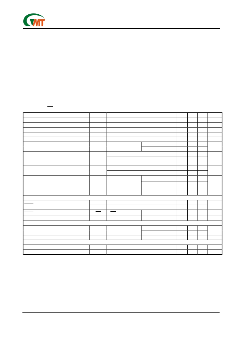
Electrical Characteristics
(V
IN
=+3.6V, V
SHDN
=V
IN
, T
A
=T
J
=+25°C, unless otherwise noted.) (Note 1)
PARAMETER
SYMBOL
V
IN
V
OUT
V
OUT
I
LIM
CONDITIONS
MIN TYP MAX UNITS
2.5
-2
V
SET
150
250
55
120
145
2
70
230
300
0.1
0.28
0.08 0.4
0.02 0.8
Input Voltage (Note 2)
Output Voltage Accuracy
Adjustable Output Voltage Range (Note 3)
Maximum Output Current
Current Limit (Note 4)
5.5
2
5.5
V
%
V
mA
mA
Variation from specified V
OUT
, I
OUT
=1mA
I
LOAD
= 0mA
I
LOAD
= 50mA
Ground Pin Current
I
Q
SET = GND
μA
I
OUT
= 1mA
I
OUT
= 50mA
I
OUT
=150mA
SET=GND, V
IN
=V
(STD)
+0.1V,to 5.5V I
OUT
= 1mA
SET tied to OUT, V
IN
=2.5V to 5.5V, I
OUT
= 1mA
Dropout Voltage (Note 5)
V
DROP
mV
Line Regulation
V
LNR
%/V
SET tied to OUT
SET = GND
Load Regulation
V
LDR
I
OUT
= 0mA to 150mA
1.0
%
Output Voltage Noise (10Hz to 100kHz)
e
n
V
IN
=4.2V,
I
OUT
=150mA
C
OUT
= 1μF
220
μV
RMS
SHUTDOWN
V
IH
V
IL
I
SHDN
Regulator enabled
Regulator shutdown
V
SHDN
= V
IN
V
OUT
= 0V
V
IN
-0.7
SHDN
Input Threshold
0.4
V
SHDN
Input Bias Current
Shutdown Supply Current
SET INPUT
T
A
= +25°C
0.003 0.1
0.2
μA
μA
I
QSHDN
T
A
= +25°C
1
T
A
= +25°C
T
A
= T
MIN
to T
MAX
T
A
= +25°C
1.225 1.25 1.275
1.25
5
SET Reference Voltage (Note 3)
V
SET
V
IN
= 2.5V to 5.5V,
I
OUT
= 1mA
V
SET
= 1.3V
V
SET Input Leakage Current (Note 3)
THERMAL PROTECTION
Thermal Shutdown Temperature
Thermal Shutdown Hysteresis
Note 1: Limits is 100% production tested at T
A
= +25°C. Low duty pulse techniques are used during test to
maintain junction temperature as close to ambient as possible.
Note 2: Guaranteed by line regulation test.
Note 3: Adjustable mode only.
Note 4: Not tested. For design purposes, the current limit should be considered 150mA minimum to 420mA maximum.
Note 5: The dropout voltage is defined as (V
IN
-V
OUT
) when V
OUT
is 100mV below the value of V
OUT
for V
IN
= V
OUT
+2V,
The performance of every G913 part, see “Typical Performance Characteristics”.
I
SET
30
nA
T
SHDN
T
SHDN
150
15
°C
°C
相關(guān)PDF資料 |
PDF描述 |
|---|---|
| G913B | 150mA Low-Dropout Linear Regulators |
| G913C | 150mA Low-Dropout Linear Regulators |
| G913D | 150mA Low-Dropout Linear Regulators |
| G914 | 150mA Low-Dropout Linear Regulators |
| G920 | 150mA Micro-power LDO Regulators |
相關(guān)代理商/技術(shù)參數(shù) |
參數(shù)描述 |
|---|---|
| G913B | 制造商:INTERPOINT 制造商全稱:INTERPOINT 功能描述:150mA Low-Dropout Linear Regulators |
| G913C | 制造商:未知廠家 制造商全稱:未知廠家 功能描述:150mA Low-Dropout Linear Regulators |
| G913D | 制造商:INTERPOINT 制造商全稱:INTERPOINT 功能描述:150mA Low-Dropout Linear Regulators |
| G913X | 制造商:未知廠家 制造商全稱:未知廠家 功能描述:5-pin. 150mA. Vo=Adjustable/Fixed(2.84/3.0/3.15/3.3V).|LDO regulator |
| G914 | 制造商:未知廠家 制造商全稱:未知廠家 功能描述:150mA Low-Dropout Linear Regulators |
發(fā)布緊急采購(gòu),3分鐘左右您將得到回復(fù)。