- 您現(xiàn)在的位置:買賣IC網(wǎng) > PDF目錄67594 > G1428F31U (Global Mixed-mode Technology Inc.) 2W Stereo Audio Amplifier PDF資料下載
參數(shù)資料
| 型號: | G1428F31U |
| 廠商: | Global Mixed-mode Technology Inc. |
| 元件分類: | 音頻放大器 |
| 英文描述: | 2W Stereo Audio Amplifier |
| 中文描述: | 2W立體聲音頻放大器 |
| 文件頁數(shù): | 6/16頁 |
| 文件大小: | 338K |
| 代理商: | G1428F31U |
Ver: 1.2
Mar 31, 2005
TEL: 886-3-5788833
http://www.gmt.com.tw
14
G1428
Global Mixed-mode Technology Inc.
Where 170k
Ω is the output impedance of the
mid-rail generator, CB is the mid-rail bypass ca-
pacitor, CI is the input coupling capacitor, RI is the
input impedance, RF is the gain setting impedance
which is on the feedback path. CB is the most im-
portant capacitor. Besides it is used to reduce the
popping, CB can also determine the rate at which
the amplifier starts up during startup or recovery
from shutdown mode.
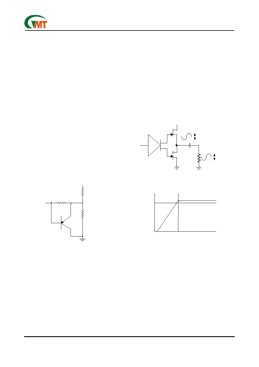
De-popping circuitry of G1428 is shown as below
Figure 2. The PNP transistor limits the voltage drop
across the 120k
Ω by slewing the internal node
slowly when power is applied. At start-up, the volt-
age at BYPASS capacitor is 0. The PNP is ON to
pull the mid-point of the bias circuit down. So the
capacitor sees a lower effective voltage, and thus
the charging is slower. This appears as a linear
ramp (while the PNP transistor is conducting), fol-
lowed by the expected exponential ramp of an R-C
circuit.
For better performance, CB is recommended to be
at least 1.5 times of input coupling capacitor CI. For
example, if using 1uF input coupling capacitor,
2.2F ceramic or tantalum low-ESR capacitors are
recommended to achieve the better THD perform-
ance.
Output coupling capacitor
G1428 can drive clean, low distortion SE output power
with gain –1V/V into headphone loads (generally 16
Ω
or 32
Ω) as in Figure 3. Please refer to Electrical
Characteristics
to see the performances. A coupling
capacitor is needed to block the dc-offset voltage, al-
lowing pure ac signals into headphone loads. Choos-
ing the coupling capacitor will also determine the -3dB
point of the high-pass filter network, as Figure 4.
fC=1/(2πRLCC)
For example, a 220F capacitor with 32
Ω headphone
load would attenuate low frequency performance be-
low 22.6Hz. So the coupling capacitor should be well
chosen to achieve the excellent bass performance
when in SE mode operation.
Bypass
VDD
100 k
Ω
100 k
Ω
120 k
Ω
Figure 2
Bypass
VDD
100 k
Ω
100 k
Ω
120 k
Ω
Figure 2
VDD
Vo(PP)
CC
RL
Figure 3
VDD
Vo(PP)
CC
RL
Figure 3
-3 dB
fc
Figure 4
-3 dB
fc
Figure 4
相關(guān)PDF資料 |
PDF描述 |
|---|---|
| G1428F31UF | 2W Stereo Audio Amplifier |
| G1430Z4T | 2W Stereo Audio Amplifier |
| G1430 | 2W Stereo Audio Amplifier |
| G1431_06 | 2W Stereo Audio Amplifier |
| G1431F2U | 2W Stereo Audio Amplifier |
相關(guān)代理商/技術(shù)參數(shù) |
參數(shù)描述 |
|---|---|
| G1428F31UF | 制造商:GMT 制造商全稱:Global Mixed-mode Technology Inc 功能描述:2W Stereo Audio Amplifier |
| G1430 | 制造商:GMT 制造商全稱:Global Mixed-mode Technology Inc 功能描述:2W Stereo Audio Amplifier |
| G1430Z4T | 制造商:GMT 制造商全稱:Global Mixed-mode Technology Inc 功能描述:2W Stereo Audio Amplifier |
| G1431 | 制造商:GMT 制造商全稱:Global Mixed-mode Technology Inc 功能描述:2W Stereo Audio Amplifier |
| G1431_06 | 制造商:GMT 制造商全稱:Global Mixed-mode Technology Inc 功能描述:2W Stereo Audio Amplifier |
發(fā)布緊急采購,3分鐘左右您將得到回復(fù)。