- 您現(xiàn)在的位置:買賣IC網(wǎng) > PDF目錄67594 > G1084T33TF (Global Mixed-mode Technology Inc.) 5A Adjustable Low-Dropout Linear Regulator PDF資料下載
參數(shù)資料
| 型號(hào): | G1084T33TF |
| 廠商: | Global Mixed-mode Technology Inc. |
| 英文描述: | 5A Adjustable Low-Dropout Linear Regulator |
| 中文描述: | 第5A可調(diào)低壓差線性穩(wěn)壓器 |
| 文件頁數(shù): | 4/11頁 |
| 文件大?。?/td> | 352K |
| 代理商: | G1084T33TF |
Ver: 1.4
Jun 14, 2007
TEL: 886-3-5788833
http://www.gmt.com.tw
2
G1084
Global Mixed-mode Technology Inc.
Absolute Maximum Ratings
(Note 1)
Operating Conditions
(Note 1)
Input Voltage . . . . . . . . . . . . . . . . . . . . . . . . . . . . . . 7V
Power Dissipation Internally Limited
(Note 2)
Maximum Junction Temperature . . . . . . . . . . . . 150°C
Storage Temperature Range . . .-65°C
≤ T
J ≤+150°C
Reflow Temperature (soldering, 10sec) . . . . . .260°C
Thermal Resistance Junction to Ambient, (
θ
JA)
TO-252
(1). . . . . . . . . . . . . . . . . . . . . . . . . . . . 85°C/W
TO-263
(1) . . . . . . . . . . . . . . . . . . . . . . . . . . . .70°C/W
TO-263T
(1) . . . . . . . . . . . . . . .. . . . . . . . . . . . 73°C/W
TO-220 No Heatsink . . . . . . . . . . . . . . . . . . 53°C/W
TO-220 with Infinite Heatsink
(2). . . . . . . . . . . 23°C/W
Thermal Resistance Junction to Case, (
θ
JC)
TO-220 . . . . . . . . . . . . . . . . . . . . . . . . . . . . . . 5°C/W
TO-252 . . . . . . . . . . . . . . . . . . . . . . . . . . . . . ..8°C/W
TO-263 . . . . . . . . . . . . . . . . . . . . . . . . . . . . . . 5°C/W
TO-263T . . . . . . . . . . . . . . . . . . . . . . . . . . . . . 5°C/W
ESD Rating (Human Body Model). . . . . . . . . . . .2kV
(VIN-VADJ) Voltage . . . . . . . . . . . . . . . . . . . . . 2.5V~5.5V
Temperature Range . . . . . . . . . . . . . .-40°C
≤T
A≤ 85°C
Note
(1): See Recommended Minimum Footprint
(2): Refer to heatsink package dimension.
Electrical Characteristics
Operating Conditions: VIN ≤ 5.5V, TA =TJ = 25°C unless otherwise specified. [Note3]
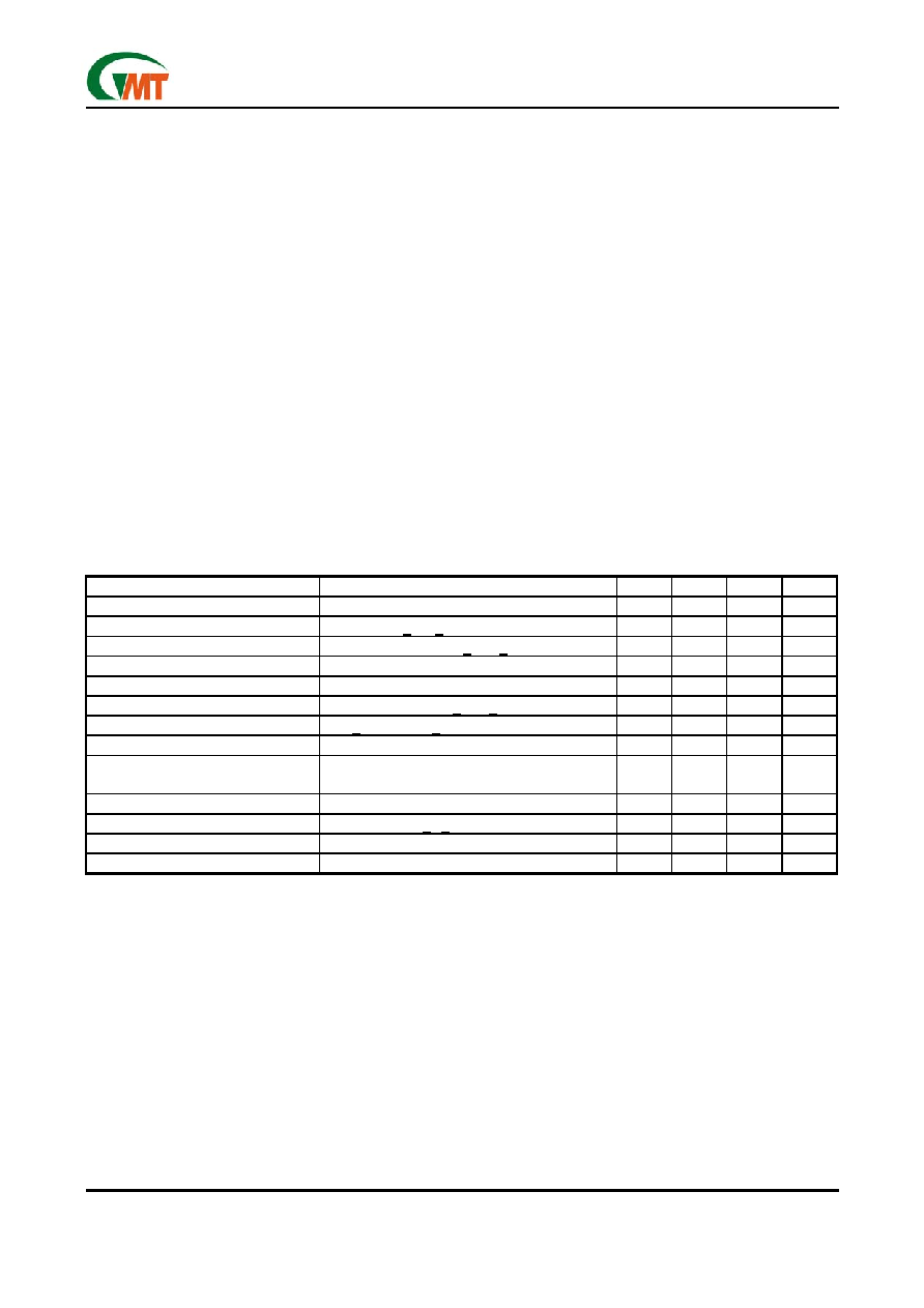
PARAMETER
CONDITION
MIN
TYP
MAX
UNIT
Reference Voltage
VIN - VOUT = 2V, IOUT = 10mA
1.225
1.250
1.275
V
Line Regulation
(VOUT + 1.5V) < VIN < 5.5V, IOUT = 10mA
---
0.5
1
%
Load Regulation
(VIN - VOUT) = 2V, 10mA < IOUT <5A
---
0.04
0.5
%
Dropout Voltage
ΔV
OUT = 2%, IOUT = 5A
---
1.3
1.5
V
Current Limit
(VIN - VOUT) = 2V
---
5.4
---
A
Adjust Pin Current Change
VIN - VOUT = 2V, 10mA < IOUT < 5A
---
0.15
---
A
Minimum Load Current
1.5V < (VIN - VOUT) < 5.25V
10
---
mA
Quiescent Current
VIN - VOUT = 2V
---
80
150
A
Ripple Rejection
f = 120Hz, COUT = 10F Tantalum,
(VIN - VOUT) = 3V, IOUT = 1A
---
45
---
dB
Temperature Stability
VIN = 4V, IO =10mA
---
0.3
---
%
RMS Output Noise (% of VOUT)
TA = 25°C, 10Hz < f < 10kHz, ILOAD = 10mA
---
0.007
---
%
Thermal Shutdown
Junction Temperature
---
150
---
°C
Thermal Shutdown Hysteresis
---
30
---
°C
Note 1:
Absolute Maximum Ratings are limits beyond which damage to the device may occur. Operating Conditions are
conditions under which the device functions but the specifications might not be guaranteed. For guaranteed specifications
and test conditions see the Electrical Characteristics.
Note2:
The maximum power dissipation is a function of the maximum junction temperature, TJmax ; total thermal resistance, θJA,
and ambient temperature TA. The maximum allowable power dissipation at any ambient temperature is Tjmax-TA / θJA. If
this dissipation is exceeded, the die temperature will rise above 150°C and IC will go into thermal shutdown.
Note3:
Low duty pulse techniques are used during test to maintain junction temperature as close to ambient as possible.
Note4:
The type of output capacitor should be tantalum or aluminum.
相關(guān)PDF資料 |
PDF描述 |
|---|---|
| G1084T33T | 5A Adjustable Low-Dropout Linear Regulator |
| G1084TU3UF | 5A Adjustable Low-Dropout Linear Regulator |
| G1084TU3U | 5A Adjustable Low-Dropout Linear Regulator |
| G1420F31Uf | 2W Stereo Audio Amplifier |
| G1420F31U | 2W Stereo Audio Amplifier |
相關(guān)代理商/技術(shù)參數(shù) |
參數(shù)描述 |
|---|---|
| G1084T41U | 制造商:GMT 制造商全稱:Global Mixed-mode Technology Inc 功能描述:5A Adjustable Low-Dropout Linear Regulator |
| G1084T42U | 制造商:GMT 制造商全稱:Global Mixed-mode Technology Inc 功能描述:5A Adjustable Low-Dropout Linear Regulator |
| G1084T43U | 制造商:GMT 制造商全稱:Global Mixed-mode Technology Inc 功能描述:5A Adjustable Low-Dropout Linear Regulator |
| G1084T43UF | 制造商:GMT 制造商全稱:Global Mixed-mode Technology Inc 功能描述:5A Adjustable Low-Dropout Linear Regulator |
| G1084T44U | 制造商:GMT 制造商全稱:Global Mixed-mode Technology Inc 功能描述:5A Adjustable Low-Dropout Linear Regulator |
發(fā)布緊急采購,3分鐘左右您將得到回復(fù)。