- 您現(xiàn)在的位置:買賣IC網(wǎng) > PDF目錄375931 > FSCM0765R (Fairchild Semiconductor Corporation) Green Mode Fairchild Power Switch (FPS) PDF資料下載
參數(shù)資料
| 型號(hào): | FSCM0765R |
| 廠商: | Fairchild Semiconductor Corporation |
| 英文描述: | Green Mode Fairchild Power Switch (FPS) |
| 中文描述: | 綠色模式飛兆半導(dǎo)體功率開關(guān)(FPS) |
| 文件頁數(shù): | 10/20頁 |
| 文件大小: | 495K |
| 代理商: | FSCM0765R |

FSCM0765R
10
Functional Description
Startup
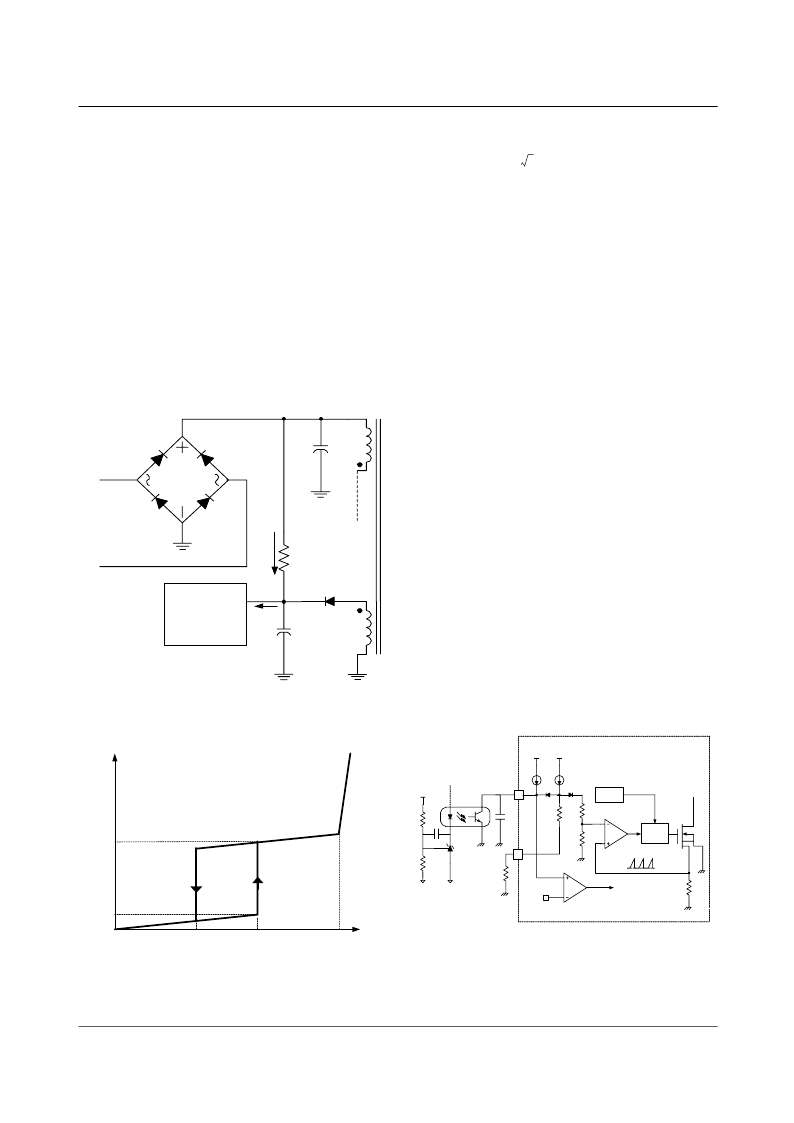
: Figure 16 shows the typical startup circuit and
transformer auxiliary winding for the FSCM0765R
application. Before the FSCM0765R begins switching, it
consumes only startup current (typically 25uA) and the
current supplied from the DC link supply current consumed
by the FPS (Icc), and charges the external capacitor (C
a
) that
is connected to the Vcc pin. When Vcc reaches start voltage
of 12V (V
START
), the
FSCM0765R begins switching, and the
current consumed by FSCM0765R increases to 3mA. Then,
the
FSCM0765R continues its normal switching operation
and the power required for this device is supplied from the
transformer auxiliary winding, unless Vcc drops below the
stop voltage of 8V (V
STOP
). To guarantee the stable operation
of the control IC, Vcc has under voltage lockout (UVLO)
with 4V hysteresis. Figure 17 shows the relation between the
current consumed by the
FPS (Icc) and the supply voltage
(Vcc).
1.
Figure 16. Startup Circuit
Figure 17. Relation Between O
perating Supply C
urrent
and Vcc Voltage
The minimum current supplied through the startup resistor is
given by
where
V
line
min
is the minimum input voltage,
V
start
is the
start voltage (12V) and
R
str
is the startup resistor. The startup
resistor should be chosen so that
I
sup
min
is larger than the
maximum startup current (40uA). If not, Vcc can not be
charged to the start voltage and FPS will fail to start up.
2. Feedback Control
: The
FSCM0765R employs current
mode control, as shown in Figure 18. An opto-coupler (such
as the H11A817A) and a shunt regulator (such as the
KA431) are typically used to implement the feedback
network. Comparing the feedback voltage with the voltage
across the Rsense resistor makes it possible to control the
switching duty cycle. When the reference pin voltage of the
KA431 exceeds the internal reference voltage of 2.5V, the
H11A817A LED current increases, thus pulling down the
feedback voltage and reducing the duty cycle. This event
typically happens when the input voltage is increased or the
output load is decreased.
2.1 Pulse-by-pulse Current Limit
: Because current mode
control is employed, the peak current through the SenseFET
is determined by the inverting input of the PWM comparator
(Vfb*) as shown in Figure 18. When the current through the
opto transistor is zero and the current limit pin (#5) is left
floating, the feedback current source (I
FB
) of 0.9mA flows
only through the internal resistor (R+2.5R=2.8k). In this
case, the cathode voltage of diode D2 and the peak drain
current have maximum values of 2.5V and 3A, respectively.
The pulse-by-pulse current limit can be adjusted using a
resistor to GND on the current limit pin (#5). The current
limit level using an external resistor (R
LIM
) is given by
:
Figure 18. Pulse Width Modulation (PWM) Circuit
FSCM0765R
Rstr
V
C C
Ca
Da
I
SUP
AC line
min
- V
line
(V
line
max
)
C
DC
I
C C
I
CC
V
CC
Vstop=8V
25uA
3mA
Vstart=12V
Vz
Power Up
Power Down
Isup
min
2 V
line
min
V
start
–
(
)
Rstr
=
I
LIM
R
3A
2.8k
Ω
+
R
LIM
------------------------------------
=
4
OSC
Vcc
Vref
I
delay
I
FB
V
SD
R
2.5R
Gate
driver
OLP
D1
D2
+
V
fb
*
-
Vfb
KA431
C
B
Vo
H11A817A
R
sense
SenseFET
6
R
LI M
0.9mA
0.3k
相關(guān)PDF資料 |
PDF描述 |
|---|---|
| FSCM0765RC | Green Mode Fairchild Power Switch (FPS) |
| FSCM0765RD | Green Mode Fairchild Power Switch (FPS) |
| FSCM0565RC | Green Mode Fairchild Power Switch (FPS) |
| FSCM0565RD | Green Mode Fairchild Power Switch (FPS) |
| FSCM0765RGWDTU | Low Cost 200 MHz Differential Receiver Amplifier; Package: SOIC; No of Pins: 8; Temperature Range: Industrial |
相關(guān)代理商/技術(shù)參數(shù) |
參數(shù)描述 |
|---|---|
| FSCM0765RC | 制造商:FAIRCHILD 制造商全稱:Fairchild Semiconductor 功能描述:Green Mode Fairchild Power Switch (FPS) |
| FSCM0765RCYDTU | 功能描述:電源開關(guān) IC - 配電 SMPS Power Switch RoHS:否 制造商:Exar 輸出端數(shù)量:1 開啟電阻(最大值):85 mOhms 開啟時(shí)間(最大值):400 us 關(guān)閉時(shí)間(最大值):20 us 工作電源電壓:3.2 V to 6.5 V 電源電流(最大值): 最大工作溫度:+ 85 C 安裝風(fēng)格:SMD/SMT 封裝 / 箱體:SOT-23-5 |
| FSCM0765RD | 功能描述:電源開關(guān) IC - 配電 SMPS Power Switch RoHS:否 制造商:Exar 輸出端數(shù)量:1 開啟電阻(最大值):85 mOhms 開啟時(shí)間(最大值):400 us 關(guān)閉時(shí)間(最大值):20 us 工作電源電壓:3.2 V to 6.5 V 電源電流(最大值): 最大工作溫度:+ 85 C 安裝風(fēng)格:SMD/SMT 封裝 / 箱體:SOT-23-5 |
| FSCM0765RG | 制造商:FAIRCHILD 制造商全稱:Fairchild Semiconductor 功能描述:Green Mode Fairchild Power Switch |
| FSCM0765RGWDTU | 功能描述:電源開關(guān) IC - 配電 SMPS POWER SWITCH POWER SWITCH GREEN RoHS:否 制造商:Exar 輸出端數(shù)量:1 開啟電阻(最大值):85 mOhms 開啟時(shí)間(最大值):400 us 關(guān)閉時(shí)間(最大值):20 us 工作電源電壓:3.2 V to 6.5 V 電源電流(最大值): 最大工作溫度:+ 85 C 安裝風(fēng)格:SMD/SMT 封裝 / 箱體:SOT-23-5 |
發(fā)布緊急采購,3分鐘左右您將得到回復(fù)。