- 您現(xiàn)在的位置:買賣IC網(wǎng) > PDF目錄375873 > FPD87392BXBVQ (National Semiconductor Corporation) +3.3V TFT-LCD Timing Controller with Dual LVDS Inputs/Dual RSDS⑩ Outputs for TFT-LCD Monitor and Notebook (SXGA/SXGA+/UXGA) PDF資料下載
參數(shù)資料
| 型號(hào): | FPD87392BXBVQ |
| 廠商: | National Semiconductor Corporation |
| 英文描述: | +3.3V TFT-LCD Timing Controller with Dual LVDS Inputs/Dual RSDS⑩ Outputs for TFT-LCD Monitor and Notebook (SXGA/SXGA+/UXGA) |
| 中文描述: | 3.3 TFT - LCD的雙LVDS輸入定時(shí)控制器/雙⑩輸出區(qū)特別職務(wù)隊(duì)的TFT - LCD顯示器和筆記本電腦(SXGA / SXGA / UXGA)下 |
| 文件頁數(shù): | 3/30頁 |
| 文件大?。?/td> | 1980K |
| 代理商: | FPD87392BXBVQ |
第1頁第2頁當(dāng)前第3頁第4頁第5頁第6頁第7頁第8頁第9頁第10頁第11頁第12頁第13頁第14頁第15頁第16頁第17頁第18頁第19頁第20頁第21頁第22頁第23頁第24頁第25頁第26頁第27頁第28頁第29頁第30頁

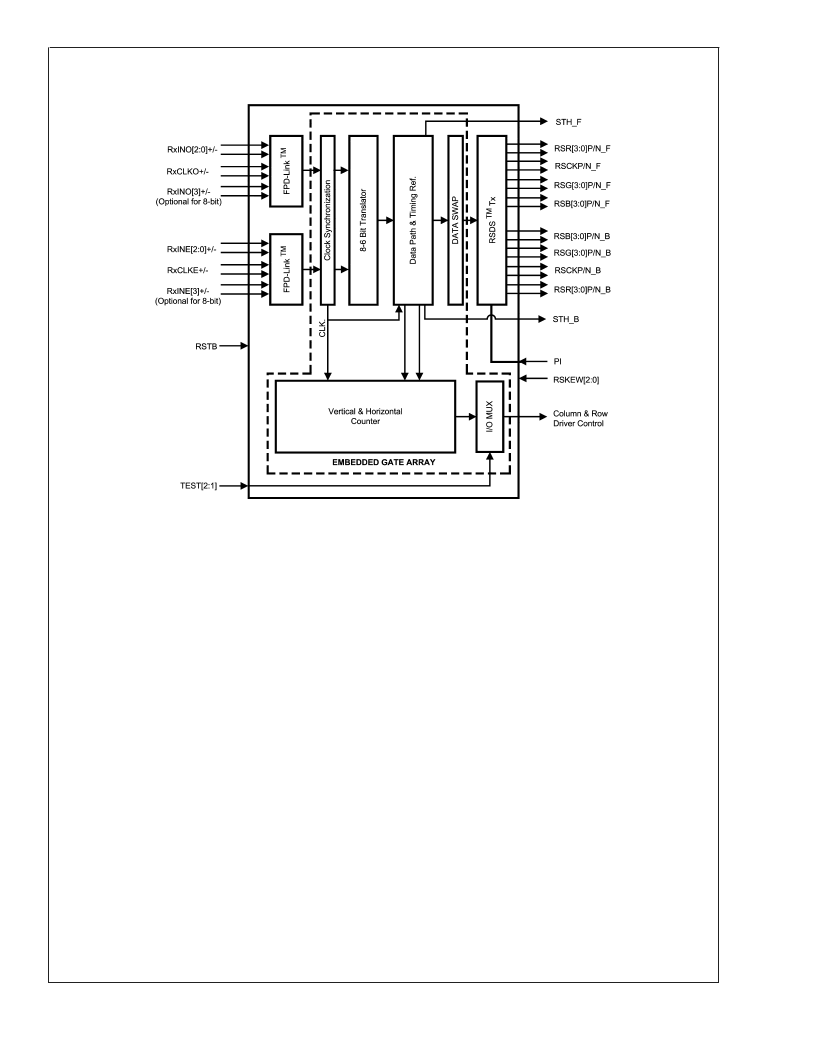
Block Diagram
Functional Description
DUAL FPD-LINK RECEIVERS
The LVDS based FPD-Link Receivers inputs video data and
control timing through 8 pairs of LVDS channels plus 2 pairs
of LVDS clocks to provide 24-bit color or use only 6 pairs of
LVDS channels plus 2 LVDS clocks to provide 18-bit color.
The video data is converted to a parallel data stream and
routed to the 8-6 bit translator.
SPREAD SPECTRUM SUPPORT
The FPD-Link receiver supports graphics controllers with
Spread Spectrum interfaces for reducing EMI. The Spread
Spectrum methods supported are Center and Down Spread.
A maximum of 2% total is supported at a frequency modu-
lation of 100kHz maximum.
8-6 BIT TRANSLATOR
8-bit data is reduced to a 6-bit data path via a time multi-
plexed dithering technique or simple truncation of the LSBs.
This function is enabled via the input control pins.
DATAPATH BLOCK AND RSDS TRANSMITTER
6(8)-bit video data (RGB) is input to the Datapath Block
supports up to an 85 MHz dual pixel rate. The data is
delayed to align the Column Driver Start Pulse (STH) with
the Column Driver data. The dual data bus (RSR[3:0]P/N,
RSG[3:0]P/N, RSB[3:0]P/N) outputs at a 170 MHz rate on 24
differential output channels. The clock is output on the
(Front, Back) RSCKP/N differential pairs. The RSDS Column
Drivers latch data on both positive and negative edges of the
clock. The swap function provides flexible RSDS data output
mappings for either Top or Bottom mount. The RSDS output
setup/hold
timings
are
also
RSKEW[2:0] input pins.
adjustable
through
the
TIMING CONTROL FUNCTION
The Timing Control function generates control to Column
Drivers, Row Drivers, and power supply. The GPOs (General
Purpose Outputs) provide for CD latch pulse, REV, and Row
Driver control generation. The General Purpose Outputs
allow the user to generate control anywhere within the frame
data. Standard Row Driver interface or Custom Row Driver
interfaces can be implemented with the GPOs (General
Purpose Outputs).
RSDS OUTPUT VOLTAGE CONTROL
The RSDS output voltage swing is controlled through an
external load resistor connected to the RPI pin. The RSDS
output signal levels can be adjusted to suit the particular
application. This is dependent on overall LCD module design
characteristics such as trace impedance, termination, etc.
The RSDS output voltage is inversely related to the RPI
value. Lower RPI values will increase the RSDS output
voltage swing and consequently overall power consumption
will also increase.
20104328
FIGURE 2. Block Diagram
F
www.national.com
3
相關(guān)PDF資料 |
PDF描述 |
|---|---|
| FPD87392 | +3.3V TFT-LCD Timing Controller with Dual LVDS Inputs/Dual RSDS⑩ Outputs for TFT-LCD Monitor and Notebook (SXGA/SXGA+/UXGA) |
| FPD87392BXB | +3.3V TFT-LCD Timing Controller with Dual LVDS Inputs/Dual RSDS⑩ Outputs for TFT-LCD Monitor and Notebook (SXGA/SXGA+/UXGA) |
| FPD94128 | 528-Ch Small Format a-Si AMLCD Controller / Column Driver with Integrated Frame Buffer |
| FPF2000 | IntelliMAX⑩ Advanced Load Management Products |
| FPF2001 | IntelliMAX⑩ Advanced Load Management Products |
相關(guān)代理商/技術(shù)參數(shù) |
參數(shù)描述 |
|---|---|
| FPD87393AMCVS/NOPB | 制造商:Texas Instruments 功能描述: |
| FPD92211A E WAF | 制造商:Texas Instruments 功能描述: |
| FPD92211SPX/NOPB | 制造商:Texas Instruments 功能描述: |
| FPD92220SNX/J7001650 | 制造商:Texas Instruments 功能描述: |
| FPD92300SNX | 制造商:Texas Instruments 功能描述: |
發(fā)布緊急采購,3分鐘左右您將得到回復(fù)。