- 您現(xiàn)在的位置:買賣IC網(wǎng) > PDF目錄375865 > FN4819 (Intersil Corporation) Synchronous-Rectified Buck MOSFET Drivers PDF資料下載
參數(shù)資料
| 型號(hào): | FN4819 |
| 廠商: | Intersil Corporation |
| 英文描述: | Synchronous-Rectified Buck MOSFET Drivers |
| 中文描述: | 同步整流降壓MOSFET驅(qū)動(dòng)器 |
| 文件頁數(shù): | 6/8頁 |
| 文件大?。?/td> | 84K |
| 代理商: | FN4819 |

6
The bootstrap device conducts when the lower MOSFET or
it’s body diode conducts and pulls the PHASE node toward
GND. While the bootstrap device conducts, a current path is
formed that refreshes the bootstrap capacitor. Since the
upper gate is driving a MOSFET, the charge removed from
the bootstrap capacitor is equivalent to the total gate charge
of the MOSFET. Therefore, the refresh power required by the
bootstrap capacitor is equivalent to the power used to
charge the gate capacitance of the MOSFET.
1
2
--
f
SW
Q
LOSS
V
PVCC
where Q
LOSS
is the total charge removed from the bootstrap
capacitor and provided to the upper gate load.
The 1.05 factor is a correction factor derived from the
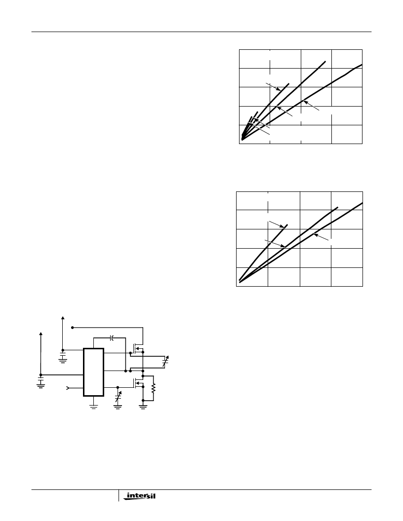
following characterization. The base circuit for characterizing
the drivers for different loading profiles and frequencies is
provided. C
U
and C
L
are the upper and lower gate load
capacitors. Decoupling capacitors [0.15
μ
F] are added to the
PVCC and VCC pins. The bootstrap capacitor value is
0.01
μ
F.
In Figure 1, C
U
and C
L
values are the same and frequency
is varied from 50kHz to 2MHz. PVCC and VCC are tied
together to a +12V supply. Curves do exceed the 800mW
cutoff, but continuous operation above this point is not
recommended.
Figure 2 shows the dissipation in the driver with 3nF loading
on both gates and each individually. Note the higher upper
gate power dissipation which is due to the bootstrap device
refresh cycle. Again PVCC and VCC are tied together and to
a +12V supply.
Test Circuit
The impact of loading on power dissipation is shown in
Figure 3. Frequency is held constant while the gate
capacitors are varied from 1nF to 5nF. VCC and PVCC are
tied together and to a +12V supply. Figures 4 through 6
show the same characterization for the HIP6603 with a +5V
supply on PVCC and VCC tied to a +12V supply.
Since both upper and lower gate capacitance can vary,
Figure 7 shows dissipation curves versus lower gate
capacitance with upper gate capacitance held constant at
three different values. These curves apply only to the
HIP6601 due to power supply configuration.
P
REFRESH
1
2
--
f
SW
Q
U
V
U
=
=
BOOT
UGATE
PHASE
LGATE
PWM
PVCC
GND
VCC
0.15
μ
F
0.15
μ
F
100k
2N7002
2N7002
C
L
0.01
μ
F
C
U
+5V OR +12V
+12V
H
1000
800
600
400
200
0
500
1000
1500
2000
P
FREQUENCY (kHz)
C
U
= C
L
= 3nF
PVCC = VCC = 12V
C
U
= C
L
= 1nF
C
U
= C
L
= 2nF
C
U
= C
L
= 4nF
C
U
= C
L
= 5nF
FIGURE 1. POWER DISSIPATION vs FREQUENCY
1000
800
600
400
200
0
500
1000
1500
2000
P
FREQUENCY (kHz)
C
U
= C
L
= 3nF
PVCC = VCC = 12V
C
U
= 3nF
C
L
= 3nF
FIGURE 2. 3nF LOADING PROFILE
HIP6601, HIP6603
相關(guān)PDF資料 |
PDF描述 |
|---|---|
| FN4819.1 | Synchronous-Rectified Buck MOSFET Drivers |
| FN4871 | Multiple Linear Power Controller with ACPI Control Interface |
| FN561 | OBSOLETE PRODUCT NO RECOMMENDED REPLACEMENT |
| FN6094 | Ultra Low ON-Resistance, Low Voltage, Single Supply, Quad SPDT (Dual DPDT) Analog Switch |
| FN7173 | Sync Separator, 50% Slice, S-H, Filter, Horizontal sync output |
相關(guān)代理商/技術(shù)參數(shù) |
參數(shù)描述 |
|---|---|
| FN4819.1 | 制造商:INTERSIL 制造商全稱:Intersil Corporation 功能描述:Synchronous-Rectified Buck MOSFET Drivers |
| FN4856 | 制造商:Vishay Siliconix 功能描述:FN4856 - Bulk |
| FN4871 | 制造商:INTERSIL 制造商全稱:Intersil Corporation 功能描述:Multiple Linear Power Controller with ACPI Control Interface |
| FN48B3 031392 | 制造商:Comair Rotron 功能描述:FAN 92X92X25MM 48VDC |
| FN48K3 039286 | 制造商:Comair Rotron 功能描述:FAN 92X92X25MM 48VDC |
發(fā)布緊急采購,3分鐘左右您將得到回復(fù)。