- 您現(xiàn)在的位置:買賣IC網(wǎng) > PDF目錄67505 > FMS3825KRC (FAIRCHILD SEMICONDUCTOR CORP) TRIPLE, PARALLEL, 8 BITS INPUT LOADING, 8-BIT DAC, PQFP48 PDF資料下載
參數(shù)資料
| 型號(hào): | FMS3825KRC |
| 廠商: | FAIRCHILD SEMICONDUCTOR CORP |
| 元件分類: | DAC |
| 英文描述: | TRIPLE, PARALLEL, 8 BITS INPUT LOADING, 8-BIT DAC, PQFP48 |
| 封裝: | LQFP-48 |
| 文件頁數(shù): | 10/11頁 |
| 文件大小: | 141K |
| 代理商: | FMS3825KRC |
FMS3810/3815/3820/3825
PRODUCT SPECIFICATION
8
REV. 1.06 9/19/00
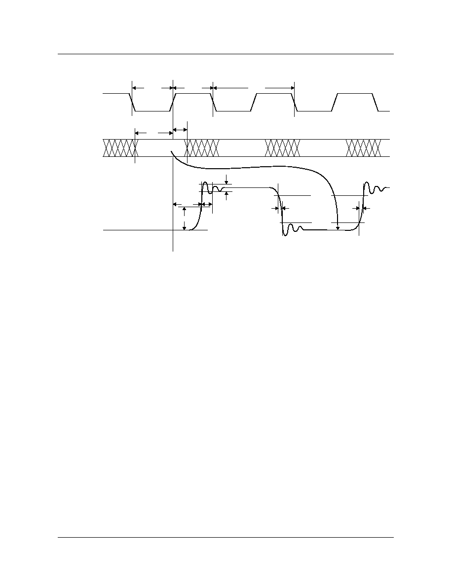
Timing Diagram
CLK
PIXEL DATA
& CONTROLS
OUTPUT
DataN
DataN+1
DataN+2
tPWL
tS
tH
50%
3%/FS
90%
10%
tD
tSET
tF
tR
tPWH
1/fS
Applications Information
Figure 4 illustrates a typical FMS3810/3815/3820/3825
interface circuit. In this example, an optional 1.2 Volt band-
gap reference is connected to the VREF output, overriding
the internal voltage reference source.
Grounding
It is important that the FMS3810/3815/3820/3825 power
supply is well-regulated and free of high-frequency noise.
Careful power supply decoupling will ensure the highest
quality video signals at the output of the circuit. The
FMS3810/3815/3820/3825 has separate analog and digital
circuits. To keep digital system noise from the
D/A converter, it is recommended that power supply voltages
(VDD) come from the system analog power source and all
ground connections (GND) be made to the analog ground
plane. Power supply pins should be individually decoupled
at the pin.
Printed Circuit Board Layout
Designing with high-performance mixed-signal circuits
demands printed circuits with ground planes. Overall system
performance is strongly inuenced by the board layout.
Capacitive coupling from digital to analog circuits may
result in poor D/A conversion. Consider the following sug-
gestions when doing the layout:
1.
Keep the critical analog traces (VREF, IREF, COMP,
IOS, IOR, IOG) as short as possible and as far as possi-
ble from all digital signals. The FMS3810/3815/3820/
3825 should be located near the board edge, close to the
analog output connectors.
2.
The power plane for the FMS3810/3815/3820/3825
should be separate from that which supplies the digital
circuitry. A single power plane should be used for all of
the VDD pins. If the power supply for the FMS3810/
3815/3820/3825 is the same as that of the system's digi-
tal circuitry, power to the FMS3810/3815/3820/3825
should be decoupled with 0.1F and 0.01F capacitors
and isolated with a ferrite bead.
3.
The ground plane should be solid, not cross-hatched.
Connections to the ground plane should have very short
leads.
4.
If the digital power supply has a dedicated power plane
layer, it should not be placed under the FMS3810/3815/
3820/3825, the voltage reference, or the analog outputs.
Capacitive coupling of digital power supply noise from
this layer to the FMS3810/3815/3820/3825 and its
related analog circuitry can have an adverse effect on
performance.
5.
CLK should be handled carefully. Jitter and noise on
this clock will degrade performance. Terminate the
clock line carefully to eliminate overshoot and ringing.
相關(guān)PDF資料 |
PDF描述 |
|---|---|
| FMS6346EMTC20X | SPECIALTY CONSUMER CIRCUIT, PDSO20 |
| FMS9874AKGC100 | 3-CH 8-BIT PROPRIETARY METHOD ADC, PARALLEL ACCESS, PQFP100 |
| FMS9874AKGC140 | 3-CH 8-BIT PROPRIETARY METHOD ADC, PARALLEL ACCESS, PQFP100 |
| FMS9875KGC100 | 3-CH 8-BIT PROPRIETARY METHOD ADC, PARALLEL ACCESS, PQFP100 |
| FMS9875KGC100X | 3-CH 8-BIT PROPRIETARY METHOD ADC, PARALLEL ACCESS, PQFP100 |
相關(guān)代理商/技術(shù)參數(shù) |
參數(shù)描述 |
|---|---|
| FMS3T148 | 制造商: 功能描述: 制造商:undefined 功能描述: |
| FMS4 | 制造商:ROHM 制造商全稱:Rohm 功能描述:General purpose (dual transistors) |
| FMS6141 | 制造商:FAIRCHILD 制造商全稱:Fairchild Semiconductor 功能描述:Low-Cost, Single-Channel 4th-Order Standard Definition Video Filter Driver |
| FMS6141_06 | 制造商:FAIRCHILD 制造商全稱:Fairchild Semiconductor 功能描述:Low-Cost, Single-Channel 4th-Order Standard Definition Video Filter Driver |
| FMS6141CS | 功能描述:有源濾波器 1-Ch 4th Order Std Video Filter Driver RoHS:否 制造商:Maxim Integrated 通道數(shù)量:1 截止頻率:150 KHz 電源電壓-最大:11 V 電源電壓-最小:4.74 V 最大工作溫度:+ 85 C 安裝風(fēng)格:Through Hole 封裝 / 箱體:PDIP N 封裝:Tube |
發(fā)布緊急采購,3分鐘左右您將得到回復(fù)。