- 您現(xiàn)在的位置:買賣IC網(wǎng) > PDF目錄67504 > FM32L278-G SPECIALTY CONSUMER CIRCUIT, PDSO14 PDF資料下載
參數(shù)資料
| 型號: | FM32L278-G |
| 元件分類: | 消費家電 |
| 英文描述: | SPECIALTY CONSUMER CIRCUIT, PDSO14 |
| 封裝: | GREEN, MS-012AB, SOIC-14 |
| 文件頁數(shù): | 6/21頁 |
| 文件大小: | 418K |
| 代理商: | FM32L278-G |
FM32L278/L276/L274/L272 - 3V I2C Companion
Rev. 3.1
July 2010
Page 14 of 21
three bytes of a write operation to set the internal
address followed by subsequent read operations.
To perform a selective read, the bus master sends out
the slave address with the LSB set to 0. This specifies
a write operation. According to the write protocol,
the bus master then sends the address bytes that are
loaded into the internal address latch. After the
FM32L27x acknowledges the address, the bus master
issues a Start condition. This simultaneously aborts
the write operation and allows the read command to
be issued with the slave address LSB set to a 1. The
operation is now a read from the current address.
Read operations are illustrated below.
Companion Write Operation
All Companion writes operate in a similar manner to
memory writes. The distinction is that a different
device ID is used and only one byte address is needed
instead of two. Figure 16 illustrates a single byte
write to this device.
Companion Read Operation
As with writes, a read operation begins with the
Slave Address. To perform a register read, the bus
master supplies a Slave Address with the LSB set to
1. This indicates that a read operation is requested.
After receiving the complete Slave Address, the
FM32L27x will begin shifting data out from the
current register address on the next clock. Auto-
increment operates for the special function registers
as with the memory address. A current address read
for the registers look exactly like the memory except
that the device ID is different.
The FM32L27x contains two separate address
registers, one for the memory address and the other
for the register address. This allows the contents of
one address register to be modified without affecting
the current address of the other register. For example,
this would allow an interrupted read to the memory
while still providing fast access to a companion
register. A subsequent memory read will then
continue from the memory address where it
previously left off, without requiring the load of a
new memory address. However, a write sequence
always requires an address to be supplied.
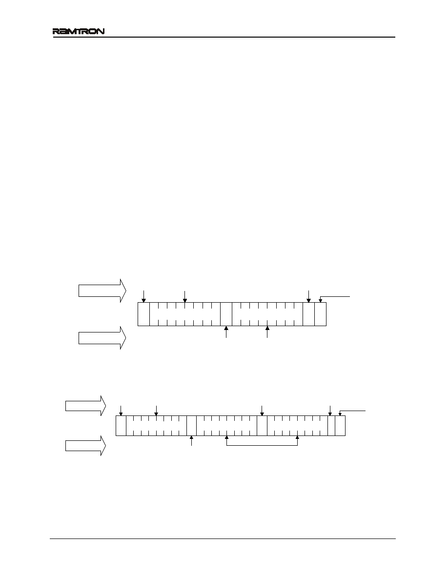
Figure 14. Current Address Memory Read
Figure 15. Sequential Memory Read
S
A
Slave Address 1
Data Byte
1 P
By Master
By FM32L27x
Start
Address
Stop
Acknowledge
No
Acknowledge
Data
Data Byte
A
Acknowledge
S
A
Slave Address
1
Data Byte
1
P
By Master
By FM32L27x
Start
Address
Stop
Acknowledge
No
Acknowledge
Data
相關(guān)PDF資料 |
PDF描述 |
|---|---|
| FM3316-GTR | SPECIALTY CONSUMER CIRCUIT, PDSO14 |
| FM3316-G | SPECIALTY CONSUMER CIRCUIT, PDSO14 |
| FM33256-GTR | SPECIALTY CONSUMER CIRCUIT, PDSO14 |
| FM33256-G | SPECIALTY CONSUMER CIRCUIT, PDSO14 |
| FM4005-G | SPECIALTY CONSUMER CIRCUIT, PDSO14 |
相關(guān)代理商/技術(shù)參數(shù) |
參數(shù)描述 |
|---|---|
| FM32L278-GTR | 功能描述:F-RAM 256K w/Pwr Mon WDT Bat Sw PF Ser Num RoHS:否 存儲容量:512 Kbit 組織:64 K x 8 接口:SPI 工作電源電壓:2 V to 3.6 V 工作溫度范圍:- 40 C to + 85 C 安裝風格:SMD/SMT 封裝 / 箱體:SOIC-8 封裝:Tube 制造商:Cypress Semiconductor |
| FM330 | 功能描述:肖特基二極管與整流器 SM Schot Bar Rect SMC,3A,30V RoHS:否 制造商:Skyworks Solutions, Inc. 產(chǎn)品:Schottky Diodes 峰值反向電壓:2 V 正向連續(xù)電流:50 mA 最大浪涌電流: 配置:Crossover Quad 恢復(fù)時間: 正向電壓下降:370 mV 最大反向漏泄電流: 最大功率耗散:75 mW 工作溫度范圍:- 65 C to + 150 C 安裝風格:SMD/SMT 封裝 / 箱體:SOT-143 封裝:Reel |
| FM330-A | 制造商:FORMOSA 制造商全稱:Formosa MS 功能描述:Chip Schottky Barrier Diodes - Silicon epitaxial planer type |
| FM330-AL | 制造商:FORMOSA 制造商全稱:Formosa MS 功能描述:Chip Schottky Barrier Diodes - Silicon epitaxial planer type |
| FM330-ALN | 制造商:FORMOSA 制造商全稱:Formosa MS 功能描述:Chip Schottky Barrier Diodes - Silicon epitaxial planer type |
發(fā)布緊急采購,3分鐘左右您將得到回復(fù)。