- 您現(xiàn)在的位置:買賣IC網(wǎng) > PDF目錄44220 > FM1901-7RD7H 1-OUTPUT 50 W DC-DC REG PWR SUPPLY MODULE PDF資料下載
參數(shù)資料
| 型號: | FM1901-7RD7H |
| 元件分類: | 電源模塊 |
| 英文描述: | 1-OUTPUT 50 W DC-DC REG PWR SUPPLY MODULE |
| 封裝: | METAL, CASE M02, MODULE |
| 文件頁數(shù): | 2/25頁 |
| 文件大小: | 569K |
| 代理商: | FM1901-7RD7H |

Cassette Style
DC-DC Converters
M Series
Edition 01/01.2001
10/25
Table 6: Output response time tr and tf. Values not applicable for modules equipped with option E.
Type of converter
tr at Po = 0 and tf at Po = Po nom tr and tf at Po = 3/4 Po nom
tr at Po = Po nom
Unit
typ
max
typ
max
typ
max
A...LM 1001-7R and C/D/LMZ 1001-7R
5
10
5
10
20
ms
A...LM 1301-7R and C/D/LMZ 1301-7R
10
20
15
30
20
40
A...LM 1501-7R and C/D/LMZ 1501-7R
5
10
20
30
60
A...LM 1601-7R and C/D/LMZ 1601-7R
15
30
25
50
40
80
A...LM 1901-7R and C/D/LMZ 1901-7R
65
130
100
200
165
330
A...LM 2320-7 and C/D/LMZ 2320-7
20
40
30
60
50
100
A...LM 2540-7 and C/D/LMZ 2540-7
15
30
20
40
35
70
A...LM 3020-7 and C/D/LMZ 3020-7
55
110
85
170
145
290
A...LM 3040-7 and C/D/LMZ 3040-7
40
80
60
120
100
200
Conditions:
R input not used. For multiple output modules the figures indicated in the table above relate to the output which reacts
slowest. All outputs are resistively loaded. Variation of the input voltage within
Ui min...Ui max does not influence the values
considerably.
Table 7: Inhibit data
Characteristics
Conditions
min
typ
max
Unit
Uinh
Inhibit input voltage to keep
Uo = on
Ui min...Ui max
–50
0.8
V DC
output voltage
Uo = off
TC min...TC max
2.4
50
I inh
Inhibit current
Uinh = 0
–60
–100
–220
A
Auxiliary Functions
i Inhibit for Remote On and Off
Note: With open i input: Output is disabled (
Uo = off).
The outputs of the module may be enabled or disabled by
means of a logic signal (TTL, CMOS, etc.) applied between
the inhibit input i and the negative pin of output 1 (Vo1–). In
systems with several units, this feature can be used, for ex-
ample, to control the activation sequence of the converters.
If the inhibit function is not required, connect the inhibit pin
2 to pin 23 to enable the outputs (active low logic, fail safe).
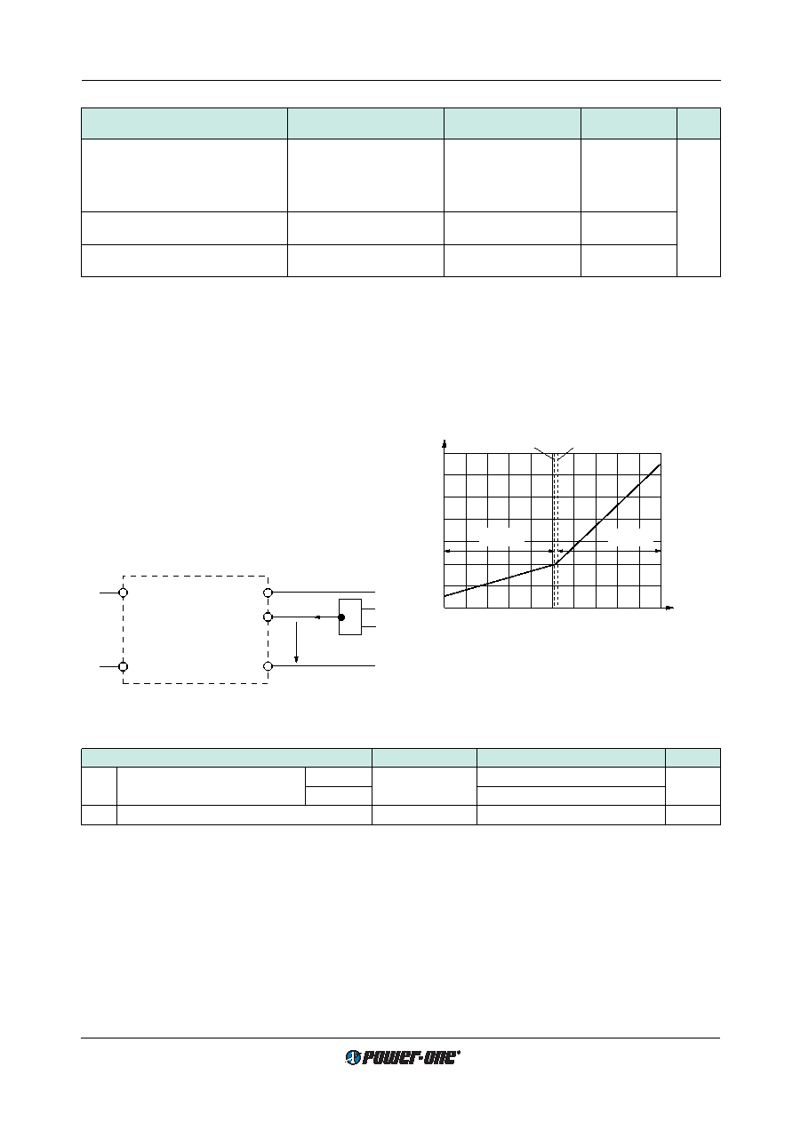
For output response refer to:
Hold-up Time and Output Re-
sponse.
Vi+
Vi–
Vo–
i
Vo+
Iinh
Uinh
06031
1.6
0.8
0
–0.8
–50
Uinh [V]
Iinh [mA]
–30
0
–10
10
30
50
2.0
1.2
0.4
–0.4
Uinh = 0.8 V
Uo = on
Uo = off
Uinh = 2.4 V
06032
Fig. 9
Definition of Uinh and Iinh.
Fig. 10
Typical inhibit current Iinh versus inhibit voltage Uinh
相關(guān)PDF資料 |
PDF描述 |
|---|---|
| FM1901-9PD4AF | 1-OUTPUT 50 W DC-DC REG PWR SUPPLY MODULE |
| FM1901-9RD5AHF | 1-OUTPUT 50 W DC-DC REG PWR SUPPLY MODULE |
| FM2320-7PV2 | 2-OUTPUT 50 W DC-DC REG PWR SUPPLY MODULE |
| FM2320-7PV3HF | 2-OUTPUT 50 W DC-DC REG PWR SUPPLY MODULE |
| FM2320-9PD2A | 2-OUTPUT 50 W DC-DC REG PWR SUPPLY MODULE |
相關(guān)代理商/技術(shù)參數(shù) |
參數(shù)描述 |
|---|---|
| FM1901-9R | 制造商:Power-One 功能描述:DCDC - Bulk |
| FM1AB-14SD-A-AA-15HU | 制造商:Hirose 功能描述: |
| FM1AB-14SD-A-AA-160HU | 制造商:Hirose 功能描述: |
| FM1AB-14SD-A-AA-18.0HU | 制造商:Hirose 功能描述:220-1751-0 EACH |
| FM1AB-14SD-A-AA-30HU | 制造商:Hirose 功能描述: |
發(fā)布緊急采購,3分鐘左右您將得到回復(fù)。