- 您現(xiàn)在的位置:買賣IC網(wǎng) > PDF目錄44176 > FM1001-7RD8AF 1-OUTPUT 50 W DC-DC REG PWR SUPPLY MODULE PDF資料下載
參數(shù)資料
| 型號(hào): | FM1001-7RD8AF |
| 元件分類: | 電源模塊 |
| 英文描述: | 1-OUTPUT 50 W DC-DC REG PWR SUPPLY MODULE |
| 封裝: | METAL, CASE M02, MODULE |
| 文件頁(yè)數(shù): | 20/25頁(yè) |
| 文件大?。?/td> | 569K |
| 代理商: | FM1001-7RD8AF |
第1頁(yè)第2頁(yè)第3頁(yè)第4頁(yè)第5頁(yè)第6頁(yè)第7頁(yè)第8頁(yè)第9頁(yè)第10頁(yè)第11頁(yè)第12頁(yè)第13頁(yè)第14頁(yè)第15頁(yè)第16頁(yè)第17頁(yè)第18頁(yè)第19頁(yè)當(dāng)前第20頁(yè)第21頁(yè)第22頁(yè)第23頁(yè)第24頁(yè)第25頁(yè)
Cassette Style
DC-DC Converters
M Series
Edition 01/01.2001
4/25
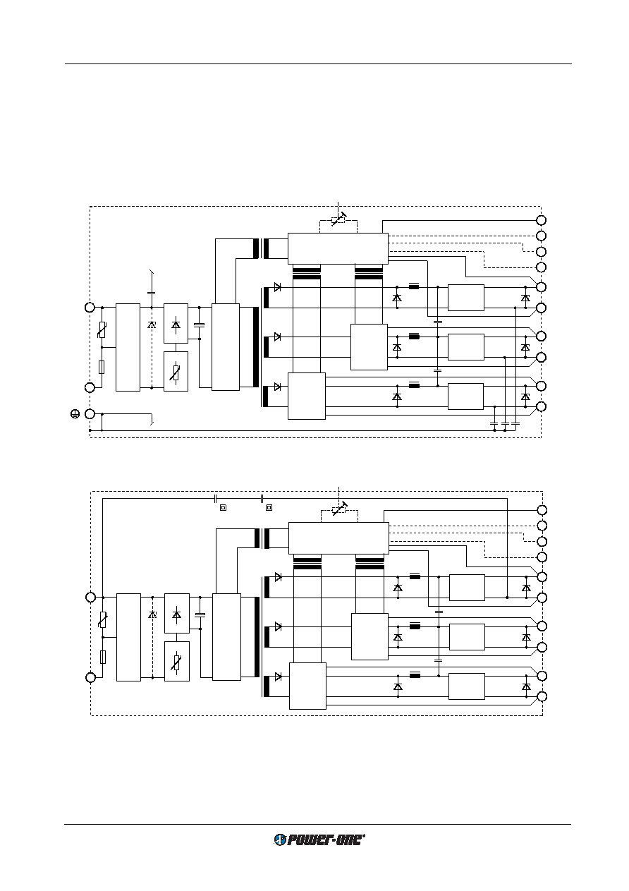
Functional Description
The input voltage is fed via an input fuse, an input filter, a
rectifier 3 and an inrush current limiter 4 to the input capaci-
tor. This capacitor sources a single transistor forward con-
verter. Each output is powered by a separate secondary
winding of the main transformer. The resultant voltages are
rectified and their ripples smoothed by a power choke and
an output filter. The control logic senses the main output
voltage
Uo1 and generates, with respect to the maximum
admissible output currents, the control signal for the pri-
mary switching transistor. This signal is fed back via a cou-
pling transformer.
The auxiliary outputs
Uo2 and Uo3 are individually regulated
by means of secondary switching transistors. Each aux-
iliary output's current is sensed using a current transformer.
If one of the outputs is driven into current limit, the other out-
puts will reduce their output voltages as well because all
output currents are controlled by the same main control cir-
cuit.
Fig. 1b
Block diagram, class II equipment (double insulation)
1 Transient suppressor diode in AM, BM, CM, FM and CMZ types.
2 Bridge rectifier in LM and LMZ, series diode in EM types.
3 Inrush current limiter (NTC) in CM, DM, EM, LM and CMZ, DMZ, LMZ types (option E: refer to the description of option E).
4 Single output modules AM...LM 1000 and CMZ...LMZ 1000 with feature R.
For output configuration please refer to table:
Pin allocation.
Fig. 1a
Block diagram, class I equipment
Input
filter
Output 1
filter
Output 3
filter
Output 2
filter
Control
circuit
Main control circuit
Control
circuit
1
Fuse
P
29
11
8
23
5
26
32
17
14
20
2
14
17
3
2
Forward
converter
approx.
70
kHz
4
CY
CMKT
Vi+
Vi–
i
D/V
R
G
03009
Input
filter
Output 1
filter
Output 3
filter
Output 2
filter
Control
circuit
Main control circuit
Control
circuit
1
Fuse
P
29
11
8
23
5
32
17
14
20
2
14
17
3
2
Forward
converter
approx.
70
kHz
4
CMKT
Vi+
Vi–
i
D/V
R
G
CY
03010
相關(guān)PDF資料 |
PDF描述 |
|---|---|
| FM1001-9PD8AH | 1-OUTPUT 50 W DC-DC REG PWR SUPPLY MODULE |
| FM1001-9RD7HF | 1-OUTPUT 50 W DC-DC REG PWR SUPPLY MODULE |
| FM1301-7PD0F | 1-OUTPUT 50 W DC-DC REG PWR SUPPLY MODULE |
| FM1301-7PD5A | 1-OUTPUT 50 W DC-DC REG PWR SUPPLY MODULE |
| FM1301-7RV3AF | 1-OUTPUT 50 W DC-DC REG PWR SUPPLY MODULE |
相關(guān)代理商/技術(shù)參數(shù) |
參數(shù)描述 |
|---|---|
| FM1001-9R | 制造商:Power-One 功能描述:DCDC - Bulk 制造商:Power-One 功能描述:M Series 50 W Single Output 5.1 V 8 A DC/DC Converter Power Supply |
| FM1002 | 制造商:未知廠家 制造商全稱:未知廠家 功能描述:CPU card chips |
| FM1004 | 制造商:未知廠家 制造商全稱:未知廠家 功能描述:CPU card chips |
| FM1008 | 制造商:BACO Controls Inc 功能描述: |
| FM1008-100DC | 制造商:未知廠家 制造商全稱:未知廠家 功能描述:NVRAM (Ferroelectric Based) |
發(fā)布緊急采購(gòu),3分鐘左右您將得到回復(fù)。