- 您現(xiàn)在的位置:買賣IC網(wǎng) > PDF目錄375799 > FIN24AMLX (FAIRCHILD SEMICONDUCTOR CORP) Low Voltage 24-Bit Bi-Directional Serializer/Deserializer with Multiple Frequency Ranges (Preliminary) PDF資料下載
參數(shù)資料
| 型號: | FIN24AMLX |
| 廠商: | FAIRCHILD SEMICONDUCTOR CORP |
| 元件分類: | 通用總線功能 |
| 英文描述: | Low Voltage 24-Bit Bi-Directional Serializer/Deserializer with Multiple Frequency Ranges (Preliminary) |
| 中文描述: | LINE TRANSCEIVER, QCC40 |
| 封裝: | 6 X 6 MM, LEAD FREE, MO-220, MLP-40 |
| 文件頁數(shù): | 8/20頁 |
| 文件大小: | 1758K |
| 代理商: | FIN24AMLX |

Preliminary
www.fairchildsemi.com
8
F
PLL Circuitry
The CKREF input signal is used to provide a reference to
the PLL. The PLL will generate internal timing signals
capable of transferring data at 26 times the incoming
CKREF signal. The output of the PLL is a Bit Clock that is
used to serialize the data. The bit clock is also sent source
synchronously with the serial data stream.
There are two ways to disable the PLL. The PLL can be
disabled by entering the Mode 0 state (S1
S2
0). The
PLL will disable immediately upon detecting a LOW on
both the S1 and S2 signals. When any of the other modes
are entered by asserting either S1 or S2 HIGH and by pro-
viding a CKREF signal the PLL will power-up and goes
through a lock sequence. One must wait the specified num-
ber of clock cycles prior to capturing valid data into the par-
allel port.
An alternate way of powering down the PLL is by stopping
the CKREF signal either HIGH or LOW. Internal circuitry
detects the lack of transitions and shuts the PLL and serial
I/O down. Internal references will not however be disabled
allowing for the PLL to power-up and re-lock in a lesser
number of clock cycles than when exiting Mode 0. When a
transition is seen on the CKREF signal the PLL will once
again be reactivated.
Application Mode Diagrams
Unidirectional Data Transfer
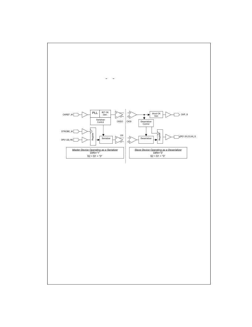
FIGURE 8. Simplified Block Diagram for Unidirectional Serializer and Deserializer
Figure 8 shows the basic operation diagram when a pair of
SerDes is configured in an unidirectional operation mode.
Master Operation:
The device will...
(Please refer to Figure 8)
1. During power-up the device will be configured as a
serializer based on the value of the DIRI signal.
2. Accept CKREF_M word clock and generate a bit clock
with embedded word boundary. This bit clock will be
sent to the slave device through the CKSO port.
3. Receive parallel data on the rising edge of
STROBE_M.
4. Generate and transmit serialized data on the DS sig-
nals which is source synchronous with CKSO.
5. Generate an embedded word clock for each strobe sig-
nal.
Slave Operation:
The device will...
1. Be configured as a deserializer at power-up based on
the value of the DIRI signal.
2. Accept an embedded word boundary bit clock on CKSI.
3. Deserialize the DS Data stream using the CKSI input
clock.
4. Write parallel data onto the DP_S port and generate
the CKP_S. CKP_S will only be generated when a valid
data word occurs.
相關(guān)PDF資料 |
PDF描述 |
|---|---|
| FIN24C | uSerDes Low Voltage 24-Bit Bi-Directional Serializer/Deserializer |
| FIN24CGFX | uSerDes Low Voltage 24-Bit Bi-Directional Serializer/Deserializer |
| FIN24CMLX | uSerDes Low Voltage 24-Bit Bi-Directional Serializer/Deserializer |
| FIN3383 | 2MM TERMINAL STRIPS |
| FIN3383MTD | 2MM TERMINAL STRIPS |
相關(guān)代理商/技術(shù)參數(shù) |
參數(shù)描述 |
|---|---|
| FIN24C | 制造商:FAIRCHILD 制造商全稱:Fairchild Semiconductor 功能描述:uSerDes⑩Low-Voltage 24-Bit Bi-Directional Serializer/Deserializer |
| FIN24C_06 | 制造商:FAIRCHILD 制造商全稱:Fairchild Semiconductor 功能描述:uSerDes⑩Low-Voltage 24-Bit Bi-Directional Serializer/Deserializer |
| FIN24CGFX | 功能描述:LVDS 接口集成電路 SerDes LV 24-Bit Bi RoHS:否 制造商:Texas Instruments 激勵器數(shù)量:4 接收機數(shù)量:4 數(shù)據(jù)速率:155.5 Mbps 工作電源電壓:5 V 最大功率耗散:1025 mW 最大工作溫度:+ 85 C 封裝 / 箱體:SOIC-16 Narrow 封裝:Reel |
| FIN24CMLX | 功能描述:LVDS 接口集成電路 SerDes LV 24-Bit Bi RoHS:否 制造商:Texas Instruments 激勵器數(shù)量:4 接收機數(shù)量:4 數(shù)據(jù)速率:155.5 Mbps 工作電源電壓:5 V 最大功率耗散:1025 mW 最大工作溫度:+ 85 C 封裝 / 箱體:SOIC-16 Narrow 封裝:Reel |
| FIN253 | 制造商:ASD (APPLIED SECURITY DESIGN) 功能描述:LIGHT FITTING ASD18 制造商:ASD (APPLIED SECURITY DESIGN) 功能描述:LIGHT, FITTING, ASD18 |
發(fā)布緊急采購,3分鐘左右您將得到回復(fù)。