- 您現(xiàn)在的位置:買(mǎi)賣(mài)IC網(wǎng) > PDF目錄375799 > FIN24A (Fairchild Semiconductor Corporation) Low Voltage 24-Bit Bi-Directional Serializer/Deserializer with Multiple Frequency Ranges (Preliminary) PDF資料下載
參數(shù)資料
| 型號(hào): | FIN24A |
| 廠商: | Fairchild Semiconductor Corporation |
| 英文描述: | Low Voltage 24-Bit Bi-Directional Serializer/Deserializer with Multiple Frequency Ranges (Preliminary) |
| 中文描述: | 低電壓24位雙向串行器/有多個(gè)頻率范圍串器(初步) |
| 文件頁(yè)數(shù): | 12/20頁(yè) |
| 文件大?。?/td> | 1758K |
| 代理商: | FIN24A |
第1頁(yè)第2頁(yè)第3頁(yè)第4頁(yè)第5頁(yè)第6頁(yè)第7頁(yè)第8頁(yè)第9頁(yè)第10頁(yè)第11頁(yè)當(dāng)前第12頁(yè)第13頁(yè)第14頁(yè)第15頁(yè)第16頁(yè)第17頁(yè)第18頁(yè)第19頁(yè)第20頁(yè)

Preliminary
www.fairchildsemi.com
12
F
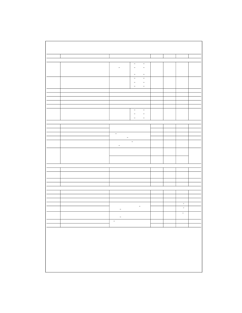
AC Electrical Characteristics
Over supply voltage and operating temperature ranges, unless otherwise specified.
Note 5:
Skew is measured from either the rising or falling edge of the clock (CKSO) relative to the center of the data bit (DSO). Both outputs should have
identical load conditions for this to be valid.
Note 6:
This jitter specification is based on the assumption that PLL has a REF Clock with cycle-to-cycle input jitter less than 2ns.
Note 7:
The power-downtime is a function of the CKREF frequency prior to CKREF being stopped HIGH or LOW and the state of the S1/S2 mode pins. The
specific number of clock cycles required for the PLL to be disabled will vary dependent upon the operating mode of the device.
Note 8:
Signals are transmitted from the serializer source synchronously. Note that in some cases data is transmitted when the clock remains at a high state.
Skew should only be measured when data and clock are transitioning at the same time. Total measured input skew would be a combination of output skew
from the serializer, load variations and ISI and jitter effects.
Note 9:
Rising edge of CKP will appear approximately 13 bit times after the falling edge of the CKP output. Falling edge of CKP will occur approximately 6 bit
times after a data transition. Variation with respect to the CKP signal is due to internal propagation delays of the device. Note that if CKREF is not equal to
STROBE for the serializer the CKP signal will not maintain a 50% Duty Cycle. The low time of CKP will remain 13 bit times.
Symbol
Serializer Electrical Characteristics
t
TCP
CKREF Clock Period
(2 MHz - 30 MHz)
Parameter
Test Conditions
Min
Typ
Max
Units
See Figure 17
S2
0
S1
1
200
T
500
ns
CKREF
STROBE
S2
1
S1
0
66.0
200
S2
1
S1
1
33.0
100
f
REF
CKREF Frequency Relative
to Strobe Frequency
CKREF
does not equal
STROBE
S2
0
S2
1
S2
1
S1
1
S1
0
S1
1
1.1 *
f
ST
5.0
15.0
30.0
MHz
t
CPWH
t
CPWL
t
CLKT
t
SPWH
t
SPWL
f
MAX
CKREF Clock High Time
CKREF Clock Low Time
LVCMOS Input Transition Time
TBD
TBD
0.5
0.5
TBD
TBD
TBD
T
T
ns
See Figure 17
STROBE Pulse Width HIGH
STROBE Pulse Width LOW
Maximum Serial Data Rate
See Figure 17
See Figure 17
CKREF x 26
5.0
5.0
52.0
ns
ns
S2
0
S1
1
130
Mb/s
S2
1
S2
1
S1
0
S1
1
130
260
390
780
Serializer AC Electrical Characteristics
t
TLH
Differential Output Rise Time (20% to 80%)
t
Differential Output Fall Time (80% to 20%)
t
STC
DP[n] Setup to STROBE
t
HTC
DP[n] Hold to STROBE
t
TCCD
Transmitter Clock Input to
Clock Output Delay
See Figure 14
0.6
0.6
0.9
0.9
ns
ns
ns
DIRI
1
2.5
See Figure 16 (f
10 MHz)
See Figure 20, DIRI
1,
CKREF
STROBE
0
ns
TBD
TBD
TBD
ns
t
SPOS
CKSO Position Relative to DS
See Figure 23, (Note 5)
CKREF Serialization Mode
See Figure 23, (Note 5)
TBD
TBD
TBD
TBD
TBD
TBD
No CKREF Serialization Mode
PLL AC Electrical Characteristics Specifications
t
JCC
CKSO Clock Out Jitter (Cycle-to-Cycle)
t
TPLLS0
Serializer Phase Lock Loop Stabilization
Time
t
TPLLD0
PLL Disable Time Loss of Clock
t
TPLLD1
PLL Power-Down Time
Deserializer AC Electrical Characteristics
t
S_DS
Serial Port Setup Time, DS-to-CKSI
t
H_DS
Serial Port Hold Time, DS-to-CKS
t
RCOP
Deserializer Clock Output (CKP OUT) Period Figure 18
t
RCOL
CKP OUT Low Time
t
RCOH
CKP OUT High Time
(Note 6)
TBD
ns
See Figure 19
1000
Cycles
See Figure 24, (Note 7)
3.0
10.0
us
See Figure 25
20.0
ns
Figure 22, (Note 8)
500
ps
Figure 22, (Note 8)
500
33.0
13a-3
ps
ns
ns
T
500
13a 3
Figure 18 (Rising Edge Strobe)
Serializer Source STROBE
CKREF
Where a
(1/f)/26 (Note 9)
Figure 18 (Rising Edge Strobe)
13a-3
13a 3
ns
t
PDV
Data Valid to CKP LOW
6a-3
6a
6a 3
ns
Where a
(1/f)/26 (Note 9)
C
L
8 pF
Figure 15
t
ROLH
t
ROHL
Output Rise Time (20% to 80%)
Output Fall time (80% to 20%)
2.5
2.5
5.0
5.0
ns
ns
相關(guān)PDF資料 |
PDF描述 |
|---|---|
| FIN24AGFX | Low Voltage 24-Bit Bi-Directional Serializer/Deserializer with Multiple Frequency Ranges (Preliminary) |
| FIN24AMLX | Low Voltage 24-Bit Bi-Directional Serializer/Deserializer with Multiple Frequency Ranges (Preliminary) |
| FIN24C | uSerDes Low Voltage 24-Bit Bi-Directional Serializer/Deserializer |
| FIN24CGFX | uSerDes Low Voltage 24-Bit Bi-Directional Serializer/Deserializer |
| FIN24CMLX | uSerDes Low Voltage 24-Bit Bi-Directional Serializer/Deserializer |
相關(guān)代理商/技術(shù)參數(shù) |
參數(shù)描述 |
|---|---|
| FIN24AC | 制造商:FAIRCHILD 制造商全稱(chēng):Fairchild Semiconductor 功能描述:USerDesTM 22-Bit Bi-Directional Serializer/Deserializer |
| FIN24AC_07 | 制造商:FAIRCHILD 制造商全稱(chēng):Fairchild Semiconductor 功能描述:22-Bit Bi-Directional Serializer/Deserializer |
| FIN24ACGFX | 功能描述:LVDS 接口集成電路 FINISHED GOOD MSL 2 RoHS:否 制造商:Texas Instruments 激勵(lì)器數(shù)量:4 接收機(jī)數(shù)量:4 數(shù)據(jù)速率:155.5 Mbps 工作電源電壓:5 V 最大功率耗散:1025 mW 最大工作溫度:+ 85 C 封裝 / 箱體:SOIC-16 Narrow 封裝:Reel |
| FIN24ACMLX | 功能描述:LVDS 接口集成電路 SerDes22-Bit Bi-Dirc Serilizr/Deserilizr RoHS:否 制造商:Texas Instruments 激勵(lì)器數(shù)量:4 接收機(jī)數(shù)量:4 數(shù)據(jù)速率:155.5 Mbps 工作電源電壓:5 V 最大功率耗散:1025 mW 最大工作溫度:+ 85 C 封裝 / 箱體:SOIC-16 Narrow 封裝:Reel |
| FIN24AGFX | 制造商:FAIRCHILD 制造商全稱(chēng):Fairchild Semiconductor 功能描述:Low Voltage 24-Bit Bi-Directional Serializer/Deserializer with Multiple Frequency Ranges (Preliminary) |
發(fā)布緊急采購(gòu),3分鐘左右您將得到回復(fù)。