- 您現(xiàn)在的位置:買賣IC網(wǎng) > PDF目錄375726 > FAN6555 (Fairchild Semiconductor Corporation) 2A DDR Bus Termination Regulator PDF資料下載
參數(shù)資料
| 型號(hào): | FAN6555 |
| 廠商: | Fairchild Semiconductor Corporation |
| 英文描述: | 2A DDR Bus Termination Regulator |
| 中文描述: | 甲DDR總線終端穩(wěn)壓器 |
| 文件頁數(shù): | 4/12頁 |
| 文件大?。?/td> | 116K |
| 代理商: | FAN6555 |

FAN6555
PRODUCT SPECIFICATION
4
REV. 1.1.3 8/4/03
Functional Description
The FAN6555 integrates two power MOSFETs that can be
used to source and sink 2A of current while maintaining a
tight voltage regulation. Using the external feedback, the
output can be regulated well within 3% or less, depending on
the external components chosen. Separate voltage supply
inputs have been added to accommodate applications with
various power supplies for the databus and power buses.
Outputs
The output voltage pins (V
address, or clock lines via an external inductor. See the
Applications section for recommendations. Output voltage
is determined by the V
CCQ
or VREF
L1
, V
L2
) are tied to the databus,
IN
inputs.
Inputs
The input voltage pins (V
output voltages (V
the VREF
IN
pin is floating, the output voltage is 50% of the
V
CCQ
input. V
CCQ
can be the reference voltage for the
databus.
CCQ
L2
or VREF
) . In the default mode, where
IN
) determine the
L1
or V
Output voltage can also be selected by forcing a voltage at
the VREF
IN
pin. In this case, the output voltage follows the
voltage at the VREF
IN
input. Simple voltage dividers can be
used in this case to produce a wide variety of output voltages
between 0.7V and V
DD
–0.7V.
VREF Input and Output
The VREF
IN
input can be used to force a voltage at the
outputs (Inputs section, above). The VREF
output pin that is driven by a small output buffer to provide
the V
REF
signal to other devices in the system. The output
buffer is capable of driving several output loads. The output
buffer can handle 3mA.
OUT
pin is an
Other Supply Voltages
Several inputs are provide for the supply voltages: PV
PV
DD2
, AV
DD1
,
CC
, and V
DD
.
The PV
DD1
and PV
DD2
provide the power supply to the
power MOSFETs. V
DD
provides the voltage supply to the
digital sections, while AV
CC
supplies the voltage for the
analog sections. Again, see the Applications section for
recommendations.
Feedback Input
The V
FB
pin is an input that can be used for closed loop
compensation. This input is derived from the voltage output.
See Application section for recommendation.
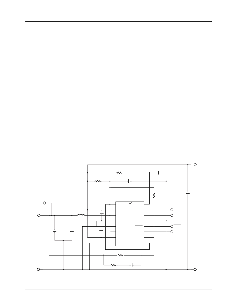
Figure 1.
16
15
14
13
12
11
10
9
U1
FAN6555
VDD
PVDD1
VL1
PGND1
PGND2
VL2
PVDD2
DGND
AVCC
VCCQ
VREFOUT
AGND
SHDN
VREFIN
VFB
VDD
1
2
3
4
5
6
7
8
R3
100k
VCCQ
VREFOUT
TPI
VTT
2.5V TO 4V
SHDN
VREFIN
GND
GND
TO SDRAMS
C7 1nF
C5
470
μ
F
C4 0.1
μ
F
R4 100k
R5 1k
C9 0.1
μ
F
R2 100
R1 100
C8 0.1
μ
F
C2
0.1
μ
F
C1
820
μ
F
F2V
OS-CON
L1 3.3
μ
H C3 0.1
μ
F
相關(guān)PDF資料 |
PDF描述 |
|---|---|
| FAN7000D | Low Power Amplifier(低功耗放大器) |
| FAN7000 | Low Power Amplifier |
| FAN7005 | 200mW Stereo Power Amplifier with Shutdown |
| FAN7005M | TV 100C 100#22D SKT RECP |
| FAN7005MU | 200mW Stereo Power Amplifier with Shutdown |
相關(guān)代理商/技術(shù)參數(shù) |
參數(shù)描述 |
|---|---|
| FAN6555M | 功能描述:DC/DC 開關(guān)控制器 2a DDR Bus Term RoHS:否 制造商:Texas Instruments 輸入電壓:6 V to 100 V 開關(guān)頻率: 輸出電壓:1.215 V to 80 V 輸出電流:3.5 A 輸出端數(shù)量:1 最大工作溫度:+ 125 C 安裝風(fēng)格: 封裝 / 箱體:CPAK |
| FAN6555M_Q | 功能描述:DC/DC 開關(guān)控制器 2a DDR Bus Term RoHS:否 制造商:Texas Instruments 輸入電壓:6 V to 100 V 開關(guān)頻率: 輸出電壓:1.215 V to 80 V 輸出電流:3.5 A 輸出端數(shù)量:1 最大工作溫度:+ 125 C 安裝風(fēng)格: 封裝 / 箱體:CPAK |
| FAN6555MX | 功能描述:DC/DC 開關(guān)控制器 2a DDR Bus Term RoHS:否 制造商:Texas Instruments 輸入電壓:6 V to 100 V 開關(guān)頻率: 輸出電壓:1.215 V to 80 V 輸出電流:3.5 A 輸出端數(shù)量:1 最大工作溫度:+ 125 C 安裝風(fēng)格: 封裝 / 箱體:CPAK |
| FAN-6-6K | 制造商:MERRIMAC 制造商全稱:MERRIMAC 功能描述:FIXED COAXIAL ATTENUATORS |
| FAN6747 | 制造商:FAIRCHILD 制造商全稱:Fairchild Semiconductor 功能描述:Highly Integrated Green-Mode PWM Controller |
發(fā)布緊急采購,3分鐘左右您將得到回復(fù)。