- 您現(xiàn)在的位置:買賣IC網(wǎng) > PDF目錄67412 > FA5500AN (FUJI ELECTRIC CO LTD) 1 A SWITCHING CONTROLLER, PDSO8 PDF資料下載
參數(shù)資料
| 型號(hào): | FA5500AN |
| 廠商: | FUJI ELECTRIC CO LTD |
| 元件分類: | 穩(wěn)壓器 |
| 英文描述: | 1 A SWITCHING CONTROLLER, PDSO8 |
| 封裝: | SO-8 |
| 文件頁(yè)數(shù): | 5/26頁(yè) |
| 文件大小: | 228K |
| 代理商: | FA5500AN |
第1頁(yè)第2頁(yè)第3頁(yè)第4頁(yè)當(dāng)前第5頁(yè)第6頁(yè)第7頁(yè)第8頁(yè)第9頁(yè)第10頁(yè)第11頁(yè)第12頁(yè)第13頁(yè)第14頁(yè)第15頁(yè)第16頁(yè)第17頁(yè)第18頁(yè)第19頁(yè)第20頁(yè)第21頁(yè)第22頁(yè)第23頁(yè)第24頁(yè)第25頁(yè)第26頁(yè)

FA5500AP/AN, FA5501AP/AN
13
Quality is our message
9. Description of PFC converter
FA5500A/FA5501A are control ICs for a power factor
correction converter using a boost type topology that
operates in critical conduction mode. The operations,
which are (1) Switching operation and (2) Power factor
correction operation, are described here with the circuit
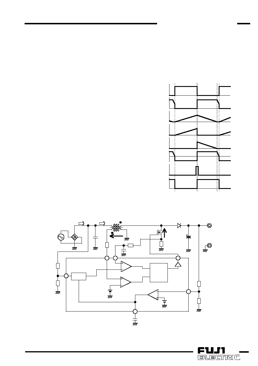
shown in Fig. 1.
(1) Switching operation
This IC operates in critical conduction current mode
and does not use a fixed frequency oscillator for
switching operation. The waveform of each part in
switching operation in steady state is shown in Fig. 2.
The operation is described in detail below:
t1. When Q1 turns on, the inductor current (IL1) rises
from zero.
t2. When the inductor current reaches up to the
threshold of the current comparator (CUR.comp.)
set by the multiplier (MUL), CUR.comp. resets R-S
flip-flop and then Q1 turns off. When Q1 is off, the
voltage of L1 reverses polarity and the L1 current
(IL1) decreases supplying a current through D1 to
the output. During this period, the voltage of the
auxiliary winding (Vsub) also reverses polarity, then
the positive voltage occurs.
t3. When IL1 reaches zero, the voltage of L1 drops
rapidly. At the same time, Vsub also drops rapidly.
t4. When Vsub drops below 1.33V (the threshold of
ZCD. comp.), the output of zero current detector
(ZCD. comp.) turns to low and sets R-S flip-flop.
Then Q1 turns on, and the next switching cycle
starts. (Back to t1)
By repeating the steps from t1 to t4, the switching
operation continues in critical conduction mode.
In the PFC converter that operates in critical
conduction mode, the switching frequency always
changes according to the instantaneous AC line
voltage. In addition, the switching frequency also
changes when the AC line voltage or the load changes.
OUT
(Q1 gate)
Q1
Vds
IL1
IQ1
ID1
CUR.comp.
output
(reset)
Vsub
ZCD.comp.
output
(set)
t1
t2
t3 t4
Fig.2
Timing chart of switching operation
AC
Iin
IL1
L1
C1
Q1
Vds
Rs
D1
Vsub
5
4
3
7
2
1
OUT
FB
2.5V
ERRAMP
COMP
ZCD.comp
CUR.comp
R
S
Q
MUL
ZCD
IS
1.5V/1.33V
Vo
MUL
FA5500A/01A
C3
Fig.1
Outline of PFC converter circuit
相關(guān)PDF資料 |
PDF描述 |
|---|---|
| FA5500AP | 1 A SWITCHING CONTROLLER, PDIP8 |
| FA5516N | 1 A SWITCHING CONTROLLER, 143 kHz SWITCHING FREQ-MAX, PDSO8 |
| FA5517N | 1 A SWITCHING CONTROLLER, 110 kHz SWITCHING FREQ-MAX, PDSO8 |
| FA5516P | 1 A SWITCHING CONTROLLER, 143 kHz SWITCHING FREQ-MAX, PDIP8 |
| FA5517P | 1 A SWITCHING CONTROLLER, 110 kHz SWITCHING FREQ-MAX, PDIP8 |
相關(guān)代理商/技術(shù)參數(shù) |
參數(shù)描述 |
|---|---|
| FA5500AP/AN | 制造商:未知廠家 制造商全稱:未知廠家 功能描述: |
| FA550-10PAK | 制造商:Black Box Corporation 功能描述:DB15 Male Transceiver Connector Kit, 10-Pack |
| FA5501AP/AN | 制造商:未知廠家 制造商全稱:未知廠家 功能描述: |
| FA5502 | 制造商:未知廠家 制造商全稱:未知廠家 功能描述:FA5502P/M is a control IC for a power factor correction system. |
| FA5502M-H1 | 制造商:Fuji Electric 功能描述: |
發(fā)布緊急采購(gòu),3分鐘左右您將得到回復(fù)。