- 您現(xiàn)在的位置:買(mǎi)賣(mài)IC網(wǎng) > PDF目錄64885 > FA5301BN (FUJI ELECTRIC CO LTD) 0.055 A SWITCHING CONTROLLER, 200 kHz SWITCHING FREQ-MAX, PDSO16 PDF資料下載
參數(shù)資料
| 型號(hào): | FA5301BN |
| 廠商: | FUJI ELECTRIC CO LTD |
| 元件分類(lèi): | 穩(wěn)壓器 |
| 英文描述: | 0.055 A SWITCHING CONTROLLER, 200 kHz SWITCHING FREQ-MAX, PDSO16 |
| 封裝: | SOP-16 |
| 文件頁(yè)數(shù): | 2/6頁(yè) |
| 文件大?。?/td> | 558K |
| 代理商: | FA5301BN |
DIS
CO
NT
INU
ED
Se
pte
mb
er
200
2
FA5301BP(N)
3
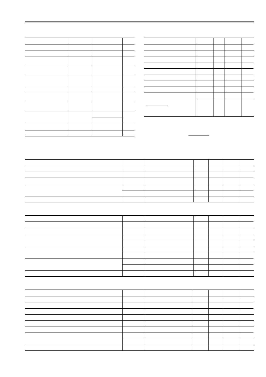
s Absolute maximum ratings
Item
Symbol
Rating
Unit
VCC
22
V
VO
22
V
IOM
5mA
VI
5V
VIS
20
V
VFB
20
V
VON/OFF
6V
VSYNC
6V
Pd
1000 (DIP-16) *1
mW
400 (SOP-16) *2
Topr
–20 to +85
°C
Tstg
–40 to +150
°C
Supply voltage
Output voltage
Error amplifier output
current
Error amplifier input
voltage
Overcurrent detection
terminal input voltage
Feedback terminal input voltage
Output ON/OFF terminal
input voltage
Synchronizing terminal
input voltage
Total power dissipation
Operating temperature
Storage temperature
Notes:
*1 Derating factor Ta > 25°C : 10.0mW/°C (on PC board)
*2 Derating factor Ta > 25°C : 4.0mW/°C (on PC board)
s Recommended operating conditions
Item
Symbol
Min.
Max.
Unit
Supply voltage
VCC
720
V
Error amplifier input voltage
VI
0
VREF-2
V
Output current
IO
20
mA
Error amplifier feedback resistor
RNF
33
k
Oscillator timing capacitor
CT
100
10,000
pF
Oscillator timing resistor
RT
8.2
220
k
Free run oscillation frequency
fOSC
1
200
kHz
Synchronized frequency
fSYNC
1
200
kHz
Frequency ratio
CSY=OV –35
–5
%
fOSC – fSYNC *3
fSYNC
–30
+10
%
CSY:
Capacitor
is connected
to GND
*3 Consider the tolerance of
fosc – fSYNC
fSYNC
s Electrical characteristics (Ta = 25
°C, VCC = 9V, RT = 47k, CT = 1000pF)
Reference voltage section
Item
Symbol
Test condition
Min.
Typ.
Max.
Unit
Output voltage
VREF
IOR = 1mA
4.75
5.00
5.25
V
Line regulation
LINE
VCC = 8 to 20V
10
25
mV
Load current regulation
LOAD
IOR = 0.1 to 2mA
10
25
mV
Output voltage variation by temperature fluctuation
VTC1
Ta = –20 to +25
°C1
%
VTC2
Ta = +25 to +85
°C1
%
Output current at output short-circuit
IOS
25
mA
Oscillator section
Item
Symbol
Test condition
Min.
Typ.
Max.
Unit
Oscillation frequency
fOSC
CT = 1,000pF, RT = 47k
20
21
22
kHz
Frequency variation by line voltage fluctuation
fdV
VCC = 8 to 20V
2
%
Frequency variation by temperature fluctuation
fdt1
Ta = +25 to –20
°C–2
+2
%
fdt2
Ta = +25 to +85
°C–2
+2
%
Input current to synchronizing signal terminal
ISYNC1
VSYNC = 1V
300
600
A
ISYNC2
VSYNC = –0.5V
–60
–300
A
Input current to synchronizing signal detection terminal
ICSY1
Pin 12 = 0V,
VSYNC = –0.5V
–65
–130
–260
A
ICSY2
Pin 12 = 1V,
VSYNC = 1V
200
400
A
Threshold voltage of synchronizing signal detection terminal
VTH CSY
0.7
1.0
V
Error amplifier section
Item
Symbol
Test condition
Min.
Typ.
Max.
Unit
Input offset voltage
VIO
–10
10
mV
Input bias current
II
1
A
Common-mode input voltage
VCM
0
VREF–2 V
Open-loop voltage gain
AV
70
95
dB
Unity-gain bandwidth
GB
0.8
MHz
Common-mode signal rejection ratio
CMRR
80
dB
Maximum output voltage
VOM+
IOM = –50
A4
V
VOM–
IOM = 50
A
0.5
V
Output sink current
IOM–
VOM = 1V
170
240
A
相關(guān)PDF資料 |
PDF描述 |
|---|---|
| FA5301P | 0.02 A SWITCHING CONTROLLER, 65 kHz SWITCHING FREQ-MAX, PDIP16 |
| FA5301N | 0.02 A SWITCHING CONTROLLER, 65 kHz SWITCHING FREQ-MAX, PDSO16 |
| FA7611CE | 0.05 A DUAL SWITCHING CONTROLLER, 200 kHz SWITCHING FREQ-MAX, PDSO16 |
| FA7611CE | 0.05 A DUAL SWITCHING CONTROLLER, 200 kHz SWITCHING FREQ-MAX, PDSO16 |
| FA7611CP | 0.05 A DUAL SWITCHING CONTROLLER, 200 kHz SWITCHING FREQ-MAX, PDIP16 |
相關(guān)代理商/技術(shù)參數(shù) |
參數(shù)描述 |
|---|---|
| FA5301BP | 制造商:FUJI 制造商全稱(chēng):Fuji Electric 功能描述:Bipolar IC For Switching Power Supply Control |
| FA5301BPN | 制造商:FUJI 制造商全稱(chēng):Fuji Electric 功能描述:Bipolar IC For Switching Power Supply Control |
| FA5301P | 制造商:未知廠家 制造商全稱(chēng):未知廠家 功能描述: |
| FA5304 | 制造商:DigitHead Inc 功能描述:CUSTOM 24" S.O. CORD 18 AWG 2 CONDUCTOR WITH TYCO CONNECTOR P/N 350547-1 AND P/ |
| FA5304AP | 制造商:FUJI 制造商全稱(chēng):Fuji Electric 功能描述:Bipolar IC For Switching Power Supply Control |
發(fā)布緊急采購(gòu),3分鐘左右您將得到回復(fù)。