- 您現(xiàn)在的位置:買賣IC網(wǎng) > PDF目錄375705 > F497 (Fujitsu Limited) 16-bit Proprietary Microcontroller CMOS PDF資料下載
參數(shù)資料
| 型號: | F497 |
| 廠商: | Fujitsu Limited |
| 英文描述: | 16-bit Proprietary Microcontroller CMOS |
| 中文描述: | 16位微控制器專有的CMOS |
| 文件頁數(shù): | 6/40頁 |
| 文件大小: | 484K |
| 代理商: | F497 |
第1頁第2頁第3頁第4頁第5頁當(dāng)前第6頁第7頁第8頁第9頁第10頁第11頁第12頁第13頁第14頁第15頁第16頁第17頁第18頁第19頁第20頁第21頁第22頁第23頁第24頁第25頁第26頁第27頁第28頁第29頁第30頁第31頁第32頁第33頁第34頁第35頁第36頁第37頁第38頁第39頁第40頁
MB90495 Series
MB90495 Series Data Sheet (Advance Information)
6 / 40
FMG EMDC June 19, 2000
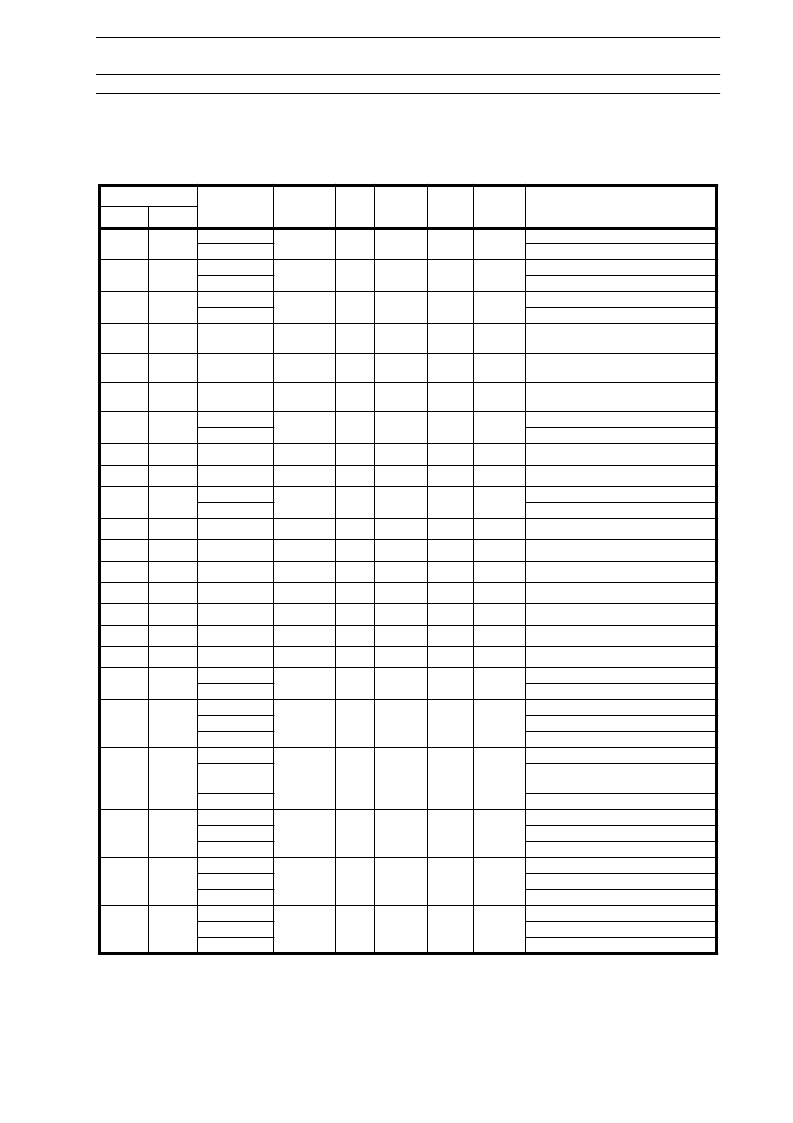
6. PIN DESCRIPTION
6.1 Pin Function
Pin No.
Pin Name
Circuit
Type
Active
Level
at RST
Priority
Function
M06
M09
2
1
P61
INT1
P62
INT2
D
H
CMOS/
TTL
High-Z
Port
General pupose IO
External Interrupt input 1
General pupose IO
External interrupt 2
General pupose IO
Inputs for A/D Converter
Dedicated power supply for A/D Con-
verter
Reference Volgate inupt for A/D Con-
verter
Dedicated power ground for A/D Con-
verter
General pupose IO
External interrupt input 0
3
2
D
H
CMOS/
TTL
High-Z
Port
4 to 11
3 to 10
P50 to P57
AN0 to AN7
E
H
CMOS
High-Z
Port
12
11
AVCC
13
12
AVR
14
13
AVSS
15
14
P60
INT0
D
H
CMOS/
TTL
High-Z
Port
16
15
X0A
A
Low frequency oscillation input
17
16
X1A
A
Low frequency oscillation output
18
17
P63
INT3
D
H
CMOS/
TTL
High-Z
Port
General purpose IO
External interrupt 3
19
18
MD0
C
H
CMOS
Mode input
20
19
RSTX
B
L
CMOS
Reset input
21
20
MD1
C
H
CMOS
Mode input
22
21
MD2
F
H
CMOS
Mode input
23
22
X0
A
High frequency oscillation input
24
23
X1
A
High frequency oscillation output
25
24
VSS
Power ground
26 to 33 25 to 32
P00 to P07
AD00 to AD07
P10 to P13
IN0 to IN3
AD08 to AD11
P14 to P17
G
H
CMOS/
TTL
High-Z
Port
General purpose IO
Addresss Data Bus
General pupose IO
Inputs for Input Captures
Address Data Bus
General pupose IO
Outputs for Programable Pulse Gener-
ators
Address Data Bus
General pupose IO
Input for 16-bit Reload Timer 0
Address Bus
General pupose IO
Output for 16-bit Reload Timer 0
Address Bus
General pupose IO
Input for 16-bit Reload Timer 1
Address Bus
34 to 37 33 to 36
G
H
CMOS/
TTL
High-Z
Port
38 to 41 37 to 40
G
H
CMOS/
TTL
High-Z
Port
PPG0 to PPG3
AD12 to AD15
P20
TIN0
A16
P21
TOT0
A17
P22
TIN1
A18
42
41
G
H
CMOS/
TTL
High-Z
Port
43
42
G
H
CMOS/
TTL
High-Z
Port
44
43
G
H
CMOS/
TTL
High-Z
Port
相關(guān)PDF資料 |
PDF描述 |
|---|---|
| F49L160BA | 16 Mbit (2M x 8/1M x 16) 3V Only CMOS Flash Memory |
| F49L160BA-70T | 16 Mbit (2M x 8/1M x 16) 3V Only CMOS Flash Memory |
| F49L160BA-90T | 16 Mbit (2M x 8/1M x 16) 3V Only CMOS Flash Memory |
| F49L160UA | 16 Mbit (2M x 8/1M x 16) 3V Only CMOS Flash Memory |
| F49L160UA-70T | 16 Mbit (2M x 8/1M x 16) 3V Only CMOS Flash Memory |
相關(guān)代理商/技術(shù)參數(shù) |
參數(shù)描述 |
|---|---|
| F-49700 | 制造商:LG Corporation 功能描述:WIRE & TERMINAL ASSY |
| F497500 | 制造商:FCI 功能描述: 制造商:Delphi Corporation 功能描述:2W_GEN3_FEM_CONN_BROWN_W |
| F-49757 | 制造商:LG Corporation 功能描述:KEYBOARD,10 KEY IR AND B |
| F49784-000 | 制造商:Elo Touch Solutions Inc 功能描述:ET1926L-7SWA-1 - Bulk |
| F-49824 | 制造商:LG Corporation 功能描述:CABINET AND |
發(fā)布緊急采購,3分鐘左右您將得到回復(fù)。