- 您現在的位置:買賣IC網 > PDF目錄362797 > EUP8051-42MIR1 (Electronic Theatre Controls, Inc.) Low Cost 1A Linear Battery Charge Controllers PDF資料下載
參數資料
| 型號: | EUP8051-42MIR1 |
| 廠商: | Electronic Theatre Controls, Inc. |
| 英文描述: | Low Cost 1A Linear Battery Charge Controllers |
| 中文描述: | 低成本1A線性電池充電控制器 |
| 文件頁數: | 11/13頁 |
| 文件大小: | 312K |
| 代理商: | EUP8051-42MIR1 |
EUP8051
Charge Inhibit Function
The TS pin can be used as charge-inhibit input. The user
can inhibit charge by connecting the TS pin to VCC or
VSS (or any level outside the V
(TS1)
to V
(TS2)
thresholds).
Applying a voltage between the V
(TS1)
and V
(TS2)
thresholds to pin
TS returns
the charger to normal
operation.
DS8051 Ver 1.2 May. 2005
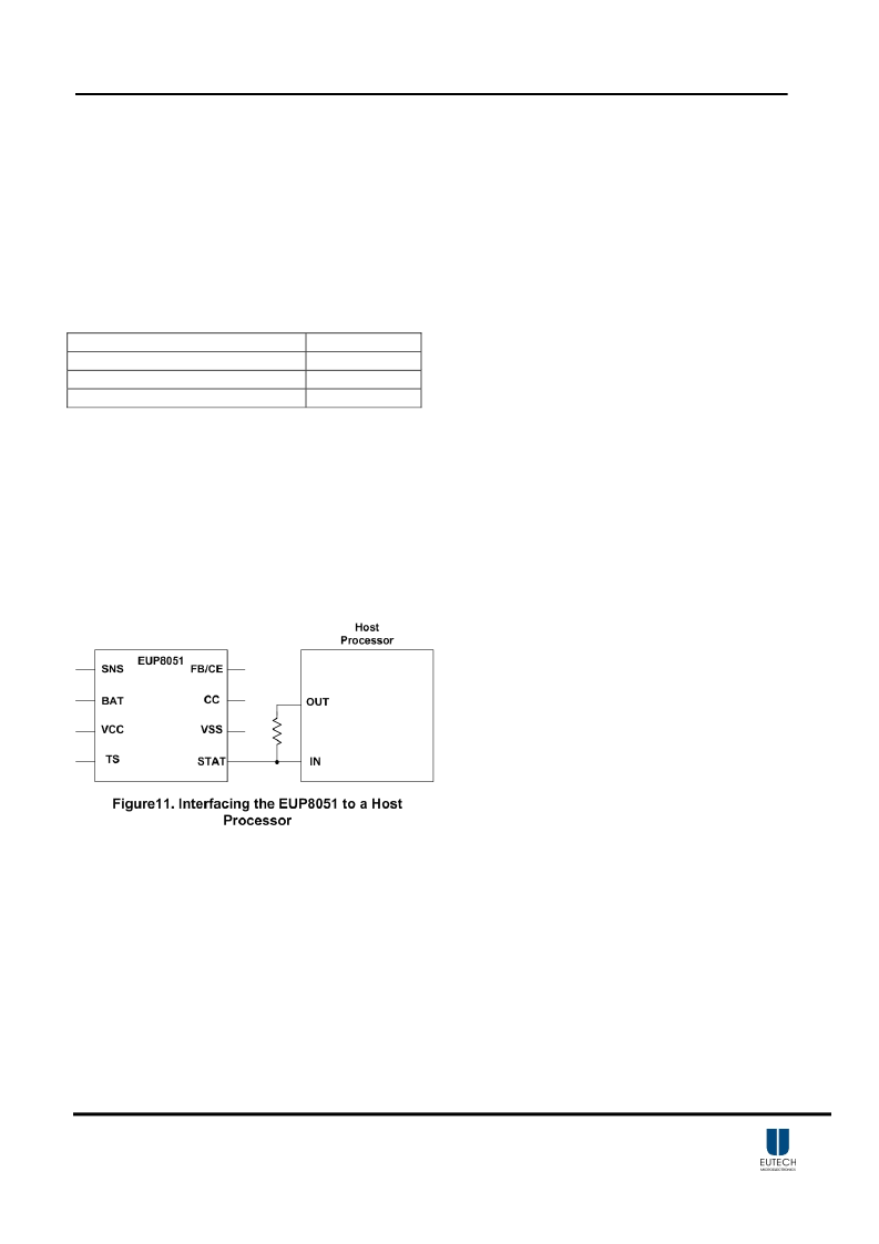
Charge Status Indication
The EUP8051 reports the status of the charger on the
3-state STAT pin. The following table summarized the
operation of the STAT pin.
Condition
Battery conditioning and charging
Charge complete(done)
Temperature fault or sleep mode
The STAT pin can be used to drive a single LED
(Figure1), dual-chip LEDs (Figure2) or for interface to a
host or system
processor (Figure11). When interfacing
the EUP8051 to a processor, the user can use an
output
port, to recognize the high-Z state of the STAT pin. In
this configuration, the user needs to read the input pin,
toggle the output port and read the STAT pin again. In a
high-Z condition, the input port always matches the
signal level on the output port.
STAT pin
High
Low
Hi-Z
Low-Power
Sleep Mode
When the input supply is disconnected, the charger
automatically enters power-saving sleep mode.
Only consuming an ultra-low 1μA in sleep mode, the
EUP8051 minimizes battery drain when it is not
charging.
Selecting Input Capacitor
In most applications, all that is needed is high-frequency
decoupling capacitor. A 0.1μF ceramic, placed in
proximity to VCC and VSS pins, works well. The
EUP8051 works with both regulated and unregulated
external dc supplies.
If a non-regulated supply
is chosen,
the supply unit should have enough capacitance to hold
up the supply voltage to the minimum required input
voltage at maximum load. If not, more capacitance must
be added to the input of the charger.
Selecting Output Capacitor
The EUP8051 does not require any output capacitor for
loop stability.
In order to maintain good AC stability in the Constant
Voltage mode, a minimum capacitance of 10μF is
recommenced to bypass the V
BAT
pin to V
SS
. This
capacitance provides compensation when there is no
battery load. In addition, the battery and interconnections
appear inductive at high frequencies. These elements are
in the control feedback loop d
mode. Therefore, the bypass capacitance may be
necessary to compensate for the inductive nature of the
battery pack.
Virtually any good quality output filter capacitor can be
used, independent of the capacitor’s minimum ESR
(Effective Series Resistance) value. The actual value of
the capacitor and its associated ESR depends on the
forward transconductance (gm) and capacitance of the
external pass transistor. A 10μF tantalum or aluminum
electrolytic capacitor at the output is usually sufficient to
ensure stability for up to a 1A output current.
Selecting An External Pass-Device (PMOS or PNP)
The EUP8051
is designed to work
with both P-channel
MOSFET or PNP transistor. The device should be chosen
to handle the required power dissipation, given the circuit
parameters, PCB layout and heat sink configuration. The
following examples illustrate the design process for
PMOS device:
uring Constant Voltage
P-Channel MOSFET
Selection steps for a P-channel MOSFET: We will use
the following conditions: V
I
=5V (with 10% supply
tolerance); I
(REG)
=1A, 4.2-V single-cell Li-Ion.
V
I
is the
input voltage to the charger and I
(REG)
is the desired
charge current. (See Figure2)
相關PDF資料 |
PDF描述 |
|---|---|
| EV0007 | 2A MP1580 Step Down Switch Mode Converter |
| EV0020 | 2A, 32V, 330KHz Step-Down Converter |
| EV0022 | Precision 6 White LED Driver Evaluation Board |
| EV0030 | 20W Class D Mono Single Ended Audio Amplifer |
| EV0033 | 1.2A Synchronous Rectified Step-Down Converter |
相關代理商/技術參數 |
參數描述 |
|---|---|
| EUP8051-42QIR1 | 制造商:EUTECH 制造商全稱:Eutech Microelectronics Inc 功能描述:Low Cost 1A Linear Battery Charge Controllers |
| EUP8051A | 制造商:EUTECH 制造商全稱:Eutech Microelectronics Inc 功能描述:Low Cost 1A Linear Battery Charge Controllers |
| EUP8051A-42MIR1 | 制造商:EUTECH 制造商全稱:Eutech Microelectronics Inc 功能描述:Low Cost 1A Linear Battery Charge Controllers |
| EUP8054 | 制造商:EUTECH 制造商全稱:Eutech Microelectronics Inc 功能描述:Standalone Linear Li-Ion Battery Charger With Thermal Regulation in ThinSOT |
| EUP8054/8054X | 制造商:未知廠家 制造商全稱:未知廠家 功能描述:Standalone Linear Li-Ion Battery Charger With Thermal Regulation in ThinSOT |
發(fā)布緊急采購,3分鐘左右您將得到回復。