參數資料
| 型號: | EPF10K100ARI240-3 |
| 廠商: | Altera |
| 文件頁數: | 23/128頁 |
| 文件大?。?/td> | 0K |
| 描述: | IC FLEX 10KA FPGA 100K 240-RQFP |
| 產品培訓模塊: | Three Reasons to Use FPGA's in Industrial Designs |
| 產品變化通告: | Package Change 30/Jun/2010 |
| 標準包裝: | 24 |
| 系列: | FLEX-10K® |
| LAB/CLB數: | 624 |
| 邏輯元件/單元數: | 4992 |
| RAM 位總計: | 24576 |
| 輸入/輸出數: | 189 |
| 門數: | 158000 |
| 電源電壓: | 3 V ~ 3.6 V |
| 安裝類型: | 表面貼裝 |
| 工作溫度: | -40°C ~ 100°C |
| 封裝/外殼: | 240-BFQFP 裸露焊盤 |
| 供應商設備封裝: | 240-RQFP(32x32) |
| 其它名稱: | 544-1251 |
第1頁第2頁第3頁第4頁第5頁第6頁第7頁第8頁第9頁第10頁第11頁第12頁第13頁第14頁第15頁第16頁第17頁第18頁第19頁第20頁第21頁第22頁當前第23頁第24頁第25頁第26頁第27頁第28頁第29頁第30頁第31頁第32頁第33頁第34頁第35頁第36頁第37頁第38頁第39頁第40頁第41頁第42頁第43頁第44頁第45頁第46頁第47頁第48頁第49頁第50頁第51頁第52頁第53頁第54頁第55頁第56頁第57頁第58頁第59頁第60頁第61頁第62頁第63頁第64頁第65頁第66頁第67頁第68頁第69頁第70頁第71頁第72頁第73頁第74頁第75頁第76頁第77頁第78頁第79頁第80頁第81頁第82頁第83頁第84頁第85頁第86頁第87頁第88頁第89頁第90頁第91頁第92頁第93頁第94頁第95頁第96頁第97頁第98頁第99頁第100頁第101頁第102頁第103頁第104頁第105頁第106頁第107頁第108頁第109頁第110頁第111頁第112頁第113頁第114頁第115頁第116頁第117頁第118頁第119頁第120頁第121頁第122頁第123頁第124頁第125頁第126頁第127頁第128頁
Altera Corporation
119
FLEX 10K Embedded Programmable Logic Device Family Data Sheet
Notes to tables:
(1)
(2)
Using an LE to register the signal may provide a lower setup time.
(3)
This parameter is specified by characterization.
ClockLock &
ClockBoost
Timing
Parameters
For the ClockLock and ClockBoost circuitry to function properly, the
incoming clock must meet certain requirements. If these specifications are
not met, the circuitry may not lock onto the incoming clock, which
generates an erroneous clock within the device. The clock generated by
the ClockLock and ClockBoost circuitry must also meet certain
specifications. If the incoming clock meets these requirements during
configuration, the ClockLock and ClockBoost circuitry will lock onto the
clock during configuration. The circuit will be ready for use immediately
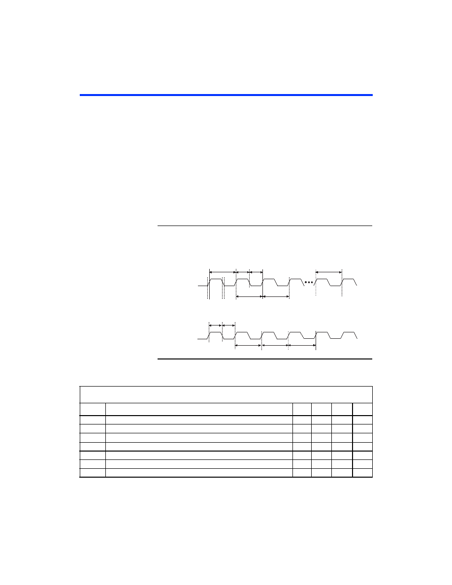
after configuration. Figure 31 illustrates the incoming and generated clock
specifications.
Figure 31. Specifications for the Incoming & Generated Clocks
The tI parameter refers to the nominal input clock period; the tO parameter refers to the
nominal output clock period.
Table 113 summarizes the ClockLock and ClockBoost parameters.
tR
tF
tCLK1
tINDUTY
tI ± fCLKDEV
tI
tI ± tINCLKSTB
tOUTDUTY
tO
tO + tJITTER
tO – tJITTER
Input
Clock
ClockLock-
Generated
Clock
Table 113. ClockLock & ClockBoost Parameters
(Part 1 of 2)
Symbol
Parameter
Min
Typ
Max
Unit
tR
Input rise time
2ns
tF
Input fall time
2ns
tINDUTY
Input duty cycle
45
55
%
fCLK1
Input clock frequency (ClockBoost clock multiplication factor equals 1)
30
80
MHz
tCLK1
Input clock period (ClockBoost clock multiplication factor equals 1)
12.5
33.3
ns
fCLK2
Input clock frequency (ClockBoost clock multiplication factor equals 2)
16
50
MHz
tCLK2
Input clock period (ClockBoost clock multiplication factor equals 2)
20
62.5
ns
相關PDF資料 |
PDF描述 |
|---|---|
| EPF10K100ARI240-3N | IC FLEX 10KA FPGA 100K 240-RQFP |
| AX1000-2BGG729 | IC FPGA AXCELERATOR 1M 729-PBGA |
| AX1000-2BG729 | IC FPGA AXCELERATOR 1M 729-PBGA |
| APA600-FGG484I | IC FPGA PROASIC+ 600K 484-FBGA |
| RSA50DTAI | CONN EDGECARD 100PS R/A .125 SLD |
相關代理商/技術參數 |
參數描述 |
|---|---|
| EPF10K100ARI240-3N | 功能描述:FPGA - 現場可編程門陣列 FPGA - Flex 10K 624 LABs 189 IOs RoHS:否 制造商:Altera Corporation 系列:Cyclone V E 柵極數量: 邏輯塊數量:943 內嵌式塊RAM - EBR:1956 kbit 輸入/輸出端數量:128 最大工作頻率:800 MHz 工作電源電壓:1.1 V 最大工作溫度:+ 70 C 安裝風格:SMD/SMT 封裝 / 箱體:FBGA-256 |
| EPF10K100B | 制造商:ALTERA 制造商全稱:Altera Corporation 功能描述:1. Enhanced Configuration Devices (EPC4, EPC8, and EPC16) Data Sheet |
| EPF10K100BFC256-1 | 制造商:Rochester Electronics LLC 功能描述:- Bulk |
| EPF10K100BFC256-1DX | 制造商:未知廠家 制造商全稱:未知廠家 功能描述:ASIC |
| EPF10K100BFC256-2 | 制造商:Rochester Electronics LLC 功能描述:- Bulk |
發(fā)布緊急采購,3分鐘左右您將得到回復。