- 您現(xiàn)在的位置:買賣IC網(wǎng) > PDF目錄299030 > EP20K100BC196-2 (ALTERA CORP) LOADABLE PLD, PBGA196 PDF資料下載
參數(shù)資料
| 型號(hào): | EP20K100BC196-2 |
| 廠商: | ALTERA CORP |
| 元件分類: | PLD |
| 英文描述: | LOADABLE PLD, PBGA196 |
| 文件頁數(shù): | 8/68頁 |
| 文件大小: | 975K |
| 代理商: | EP20K100BC196-2 |
第1頁第2頁第3頁第4頁第5頁第6頁第7頁當(dāng)前第8頁第9頁第10頁第11頁第12頁第13頁第14頁第15頁第16頁第17頁第18頁第19頁第20頁第21頁第22頁第23頁第24頁第25頁第26頁第27頁第28頁第29頁第30頁第31頁第32頁第33頁第34頁第35頁第36頁第37頁第38頁第39頁第40頁第41頁第42頁第43頁第44頁第45頁第46頁第47頁第48頁第49頁第50頁第51頁第52頁第53頁第54頁第55頁第56頁第57頁第58頁第59頁第60頁第61頁第62頁第63頁第64頁第65頁第66頁第67頁第68頁
16
4317K–AVR–03/2013
AT90PWM2/3/2B/3B
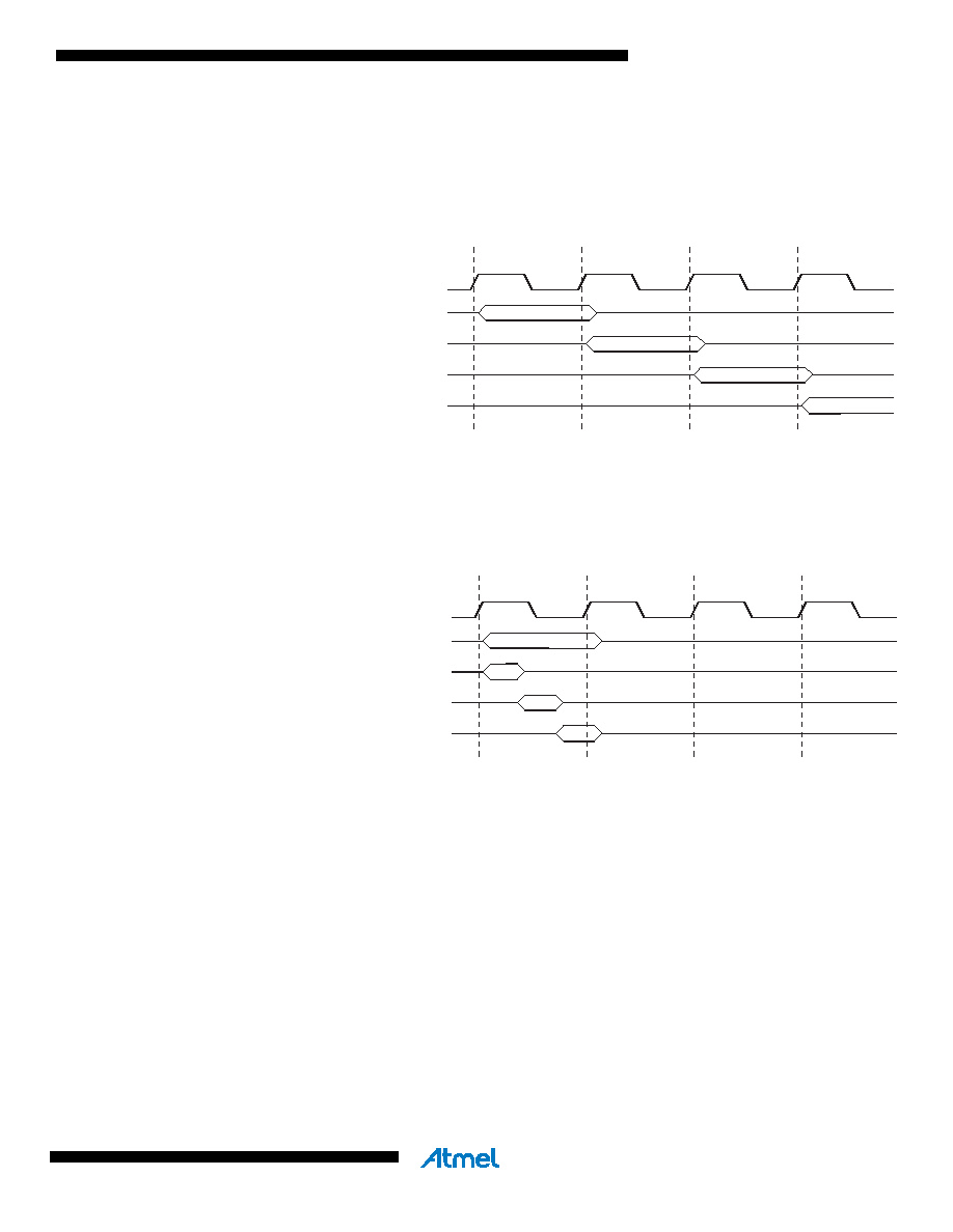
Figure 5-4 shows the parallel instruction fetches and instruction executions enabled by the Har-
vard architecture and the fast-access Register File concept. This is the basic pipelining concept
to obtain up to 1 MIPS per MHz with the corresponding unique results for functions per cost,
functions per clocks, and functions per power-unit.
Figure 5-4.
The Parallel Instruction Fetches and Instruction Executions
Figure 5-5 shows the internal timing concept for the Register File. In a single clock cycle an ALU
operation using two register operands is executed, and the result is stored back to the destina-
tion register.
Figure 5-5.
Single Cycle ALU Operation
5.8
Reset and Interrupt Handling
The AVR provides several different interrupt sources. These interrupts and the separate Reset
Vector each have a separate program vector in the program memory space. All interrupts are
assigned individual enable bits which must be written logic one together with the Global Interrupt
Enable bit in the Status Register in order to enable the interrupt. Depending on the Program
Counter value, interrupts may be automatically disabled when Boot Lock bits BLB02 or BLB12
are programmed. This feature improves software security. See the section “Memory Program-
ming” on page 280 for details.
The lowest addresses in the program memory space are by default defined as the Reset and
Interrupt Vectors. The complete list of vectors is shown in “Interrupts” on page 57. The list also
determines the priority levels of the different interrupts. The lower the address the higher is the
priority level. RESET has the highest priority, and next is PSC2 CAPT – the PSC2 Capture
Event. The Interrupt Vectors can be moved to the start of the Boot Flash section by setting the
IVSEL bit in the MCU Control Register (MCUCR). Refer to “Interrupts” on page 57 for more infor-
mation. The Reset Vector can also be moved to the start of the Boot Flash section by
clk
1st Instruction Fetch
1st Instruction Execute
2nd Instruction Fetch
2nd Instruction Execute
3rd Instruction Fetch
3rd Instruction Execute
4th Instruction Fetch
T1
T2
T3
T4
CPU
Total Execution Time
Register Operands Fetch
ALU Operation Execute
Result Write Back
T1
T2
T3
T4
clk
CPU
相關(guān)PDF資料 |
PDF描述 |
|---|---|
| EP20K100BC196-3 | LOADABLE PLD, PBGA196 |
| EP20K100BI196-1 | LOADABLE PLD, PBGA196 |
| EP20K100BI196-2 | LOADABLE PLD, PBGA196 |
| EP20K100BI196-3 | LOADABLE PLD, PBGA196 |
| EP20K100BC324-1 | LOADABLE PLD, PBGA324 |
相關(guān)代理商/技術(shù)參數(shù) |
參數(shù)描述 |
|---|---|
| EP20K100BC356-1 | 功能描述:FPGA - 現(xiàn)場可編程門陣列 CPLD - APEX 20K 416 Macro 252 IOs RoHS:否 制造商:Altera Corporation 系列:Cyclone V E 柵極數(shù)量: 邏輯塊數(shù)量:943 內(nèi)嵌式塊RAM - EBR:1956 kbit 輸入/輸出端數(shù)量:128 最大工作頻率:800 MHz 工作電源電壓:1.1 V 最大工作溫度:+ 70 C 安裝風(fēng)格:SMD/SMT 封裝 / 箱體:FBGA-256 |
| EP20K100BC356-1ES | 制造商:未知廠家 制造商全稱:未知廠家 功能描述:FPGA |
| EP20K100BC356-1V | 制造商:Rochester Electronics LLC 功能描述:- Bulk |
| EP20K100BC356-2 | 功能描述:FPGA - 現(xiàn)場可編程門陣列 CPLD - APEX 20K 416 Macro 252 IOs RoHS:否 制造商:Altera Corporation 系列:Cyclone V E 柵極數(shù)量: 邏輯塊數(shù)量:943 內(nèi)嵌式塊RAM - EBR:1956 kbit 輸入/輸出端數(shù)量:128 最大工作頻率:800 MHz 工作電源電壓:1.1 V 最大工作溫度:+ 70 C 安裝風(fēng)格:SMD/SMT 封裝 / 箱體:FBGA-256 |
| EP20K100BC356-2ES | 制造商:未知廠家 制造商全稱:未知廠家 功能描述:FPGA |
發(fā)布緊急采購,3分鐘左右您將得到回復(fù)。