- 您現(xiàn)在的位置:買賣IC網(wǎng) > PDF目錄362739 > EP1K30 (Electronic Theatre Controls, Inc.) Programmable Logic Device Family PDF資料下載
參數(shù)資料
| 型號: | EP1K30 |
| 廠商: | Electronic Theatre Controls, Inc. |
| 英文描述: | Programmable Logic Device Family |
| 中文描述: | 可編程邏輯器件系列 |
| 文件頁數(shù): | 48/86頁 |
| 文件大小: | 992K |
| 代理商: | EP1K30 |
第1頁第2頁第3頁第4頁第5頁第6頁第7頁第8頁第9頁第10頁第11頁第12頁第13頁第14頁第15頁第16頁第17頁第18頁第19頁第20頁第21頁第22頁第23頁第24頁第25頁第26頁第27頁第28頁第29頁第30頁第31頁第32頁第33頁第34頁第35頁第36頁第37頁第38頁第39頁第40頁第41頁第42頁第43頁第44頁第45頁第46頁第47頁當前第48頁第49頁第50頁第51頁第52頁第53頁第54頁第55頁第56頁第57頁第58頁第59頁第60頁第61頁第62頁第63頁第64頁第65頁第66頁第67頁第68頁第69頁第70頁第71頁第72頁第73頁第74頁第75頁第76頁第77頁第78頁第79頁第80頁第81頁第82頁第83頁第84頁第85頁第86頁
48
Altera Corporation
ACEX 1K Programmable Logic Device Family Data Sheet
Notes to tables:
(1)
See the
Operating Requirements for Altera Devices Data Sheet
.
(2)
Minimum DC input voltage is –0.5 V. During transitions, the inputs may undershoot to –2.0 V for input currents
less than 100 mA and periods shorter than 20 ns.
(3)
Numbers in parentheses are for industrial-temperature-range devices.
(4)
Maximum V
CC
rise time is 100 ms, and V
CC
must rise monotonically.
(5)
All pins, including dedicated inputs, clock, I/ O, and JTAG pins, may be driven before V
CCINT
and V
CCIO
are
powered.
(6)
Typical values are for T
A
= 25
°
C, V
CCINT
= 2.5 V, and V
CCIO
= 2.5 V or 3.3 V.
(7)
These values are specified under the ACEX 1K Recommended Operating Conditions shown in Table 19 on page 46.
(8)
The ACEX 1K input buffers are compatible with 2.5-V, 3.3-V (LVTTL and LVCMOS), and 5.0-V TTL and CMOS
signals. Additionally, the input buffers are 3.3-V PCI compliant when V
CCIO
and V
CCINT
meet the relationship
shown in
Figure 22
.
(9)
The I
OH
parameter refers to high-level TTL, PCI, or CMOS output current.
(10) The I
OL
parameter refers to low-level TTL, PCI, or CMOS output current. This parameter applies to open-drain pins
as well as output pins.
(11) This value is specified for normal device operation. The value may vary during power-up.
(12) This parameter applies to -1 speed grade commercial temperature devices and -2 speed grade industrial
temperature devices.
(13) Pin pull-up resistance values will be lower if the pin is driven higher than V
CCIO
by an external source.
(14) Capacitance is sample-tested only.
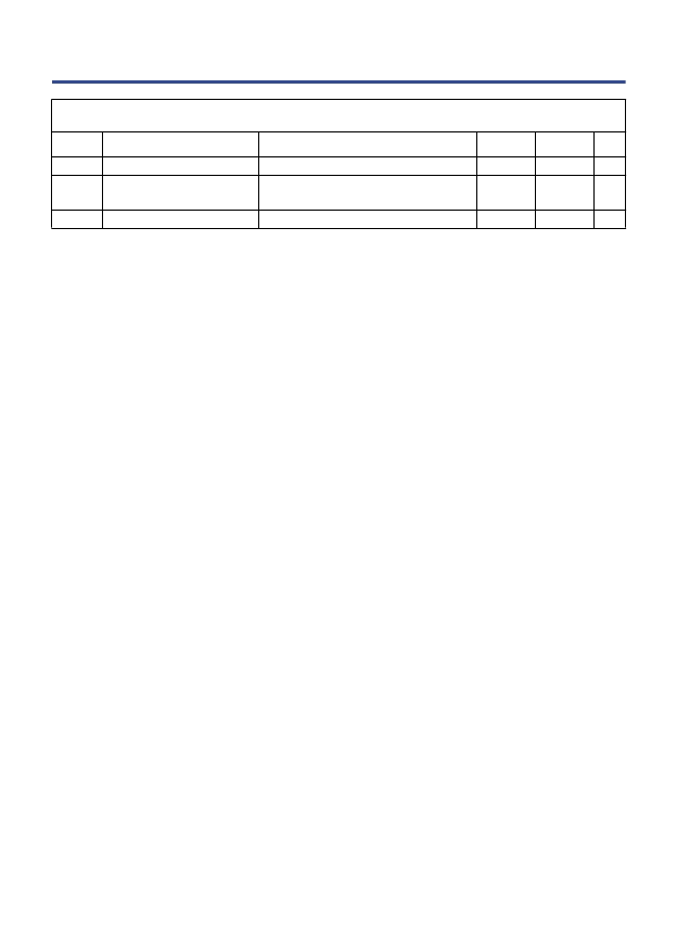
Table 21. ACEX 1K Device Capacitance
Note (14)
Symbol
Parameter
Conditions
Min
Max
Unit
C
IN
C
INCLK
Input capacitance
Input capacitance on
dedicated clock pin
Output capacitance
V
IN
= 0 V, f = 1.0 MHz
V
IN
= 0 V, f = 1.0 MHz
10
12
pF
pF
C
OUT
V
OUT
= 0 V, f = 1.0 MHz
10
pF
相關(guān)PDF資料 |
PDF描述 |
|---|---|
| EP1K50 | Programmable Logic Device Family |
| EP1S60B1508C5ES | Stratix Device Family Data Sheet |
| EP1S10B1508C6ES | Stratix Device Family Data Sheet |
| EP1S80F1508I5ES | Stratix Device Family Data Sheet |
| EP1S80F1508I6ES | Stratix Device Family Data Sheet |
相關(guān)代理商/技術(shù)參數(shù) |
參數(shù)描述 |
|---|---|
| EP1K30FC256-1 | 功能描述:FPGA - 現(xiàn)場可編程門陣列 FPGA - ACEX 1K 216 LABs 171 IOs RoHS:否 制造商:Altera Corporation 系列:Cyclone V E 柵極數(shù)量: 邏輯塊數(shù)量:943 內(nèi)嵌式塊RAM - EBR:1956 kbit 輸入/輸出端數(shù)量:128 最大工作頻率:800 MHz 工作電源電壓:1.1 V 最大工作溫度:+ 70 C 安裝風(fēng)格:SMD/SMT 封裝 / 箱體:FBGA-256 |
| EP1K30FC256-1N | 功能描述:FPGA - 現(xiàn)場可編程門陣列 FPGA - ACEX 1K 216 LABs 171 IOs RoHS:否 制造商:Altera Corporation 系列:Cyclone V E 柵極數(shù)量: 邏輯塊數(shù)量:943 內(nèi)嵌式塊RAM - EBR:1956 kbit 輸入/輸出端數(shù)量:128 最大工作頻率:800 MHz 工作電源電壓:1.1 V 最大工作溫度:+ 70 C 安裝風(fēng)格:SMD/SMT 封裝 / 箱體:FBGA-256 |
| EP1K30FC256-2 | 功能描述:FPGA - 現(xiàn)場可編程門陣列 FPGA - ACEX 1K 216 LABs 171 IOs RoHS:否 制造商:Altera Corporation 系列:Cyclone V E 柵極數(shù)量: 邏輯塊數(shù)量:943 內(nèi)嵌式塊RAM - EBR:1956 kbit 輸入/輸出端數(shù)量:128 最大工作頻率:800 MHz 工作電源電壓:1.1 V 最大工作溫度:+ 70 C 安裝風(fēng)格:SMD/SMT 封裝 / 箱體:FBGA-256 |
| EP1K30FC256-2N | 功能描述:FPGA - 現(xiàn)場可編程門陣列 FPGA - ACEX 1K 216 LABs 171 IOs RoHS:否 制造商:Altera Corporation 系列:Cyclone V E 柵極數(shù)量: 邏輯塊數(shù)量:943 內(nèi)嵌式塊RAM - EBR:1956 kbit 輸入/輸出端數(shù)量:128 最大工作頻率:800 MHz 工作電源電壓:1.1 V 最大工作溫度:+ 70 C 安裝風(fēng)格:SMD/SMT 封裝 / 箱體:FBGA-256 |
| EP1K30FC256-3 | 功能描述:FPGA - 現(xiàn)場可編程門陣列 FPGA - ACEX 1K 216 LABs 171 IOs RoHS:否 制造商:Altera Corporation 系列:Cyclone V E 柵極數(shù)量: 邏輯塊數(shù)量:943 內(nèi)嵌式塊RAM - EBR:1956 kbit 輸入/輸出端數(shù)量:128 最大工作頻率:800 MHz 工作電源電壓:1.1 V 最大工作溫度:+ 70 C 安裝風(fēng)格:SMD/SMT 封裝 / 箱體:FBGA-256 |
發(fā)布緊急采購,3分鐘左右您將得到回復(fù)。