- 您現(xiàn)在的位置:買賣IC網(wǎng) > PDF目錄362736 > EP1C6Q240C8 (Altera Corporation) Cyclone FPGA Family PDF資料下載
參數(shù)資料
| 型號(hào): | EP1C6Q240C8 |
| 廠商: | Altera Corporation |
| 英文描述: | Cyclone FPGA Family |
| 中文描述: | 氣旋FPGA系列 |
| 文件頁(yè)數(shù): | 53/94頁(yè) |
| 文件大小: | 1138K |
| 代理商: | EP1C6Q240C8 |
第1頁(yè)第2頁(yè)第3頁(yè)第4頁(yè)第5頁(yè)第6頁(yè)第7頁(yè)第8頁(yè)第9頁(yè)第10頁(yè)第11頁(yè)第12頁(yè)第13頁(yè)第14頁(yè)第15頁(yè)第16頁(yè)第17頁(yè)第18頁(yè)第19頁(yè)第20頁(yè)第21頁(yè)第22頁(yè)第23頁(yè)第24頁(yè)第25頁(yè)第26頁(yè)第27頁(yè)第28頁(yè)第29頁(yè)第30頁(yè)第31頁(yè)第32頁(yè)第33頁(yè)第34頁(yè)第35頁(yè)第36頁(yè)第37頁(yè)第38頁(yè)第39頁(yè)第40頁(yè)第41頁(yè)第42頁(yè)第43頁(yè)第44頁(yè)第45頁(yè)第46頁(yè)第47頁(yè)第48頁(yè)第49頁(yè)第50頁(yè)第51頁(yè)第52頁(yè)當(dāng)前第53頁(yè)第54頁(yè)第55頁(yè)第56頁(yè)第57頁(yè)第58頁(yè)第59頁(yè)第60頁(yè)第61頁(yè)第62頁(yè)第63頁(yè)第64頁(yè)第65頁(yè)第66頁(yè)第67頁(yè)第68頁(yè)第69頁(yè)第70頁(yè)第71頁(yè)第72頁(yè)第73頁(yè)第74頁(yè)第75頁(yè)第76頁(yè)第77頁(yè)第78頁(yè)第79頁(yè)第80頁(yè)第81頁(yè)第82頁(yè)第83頁(yè)第84頁(yè)第85頁(yè)第86頁(yè)第87頁(yè)第88頁(yè)第89頁(yè)第90頁(yè)第91頁(yè)第92頁(yè)第93頁(yè)第94頁(yè)
Altera Corporation
53
Preliminary Information
Cyclone FPGA Family Data Sheet
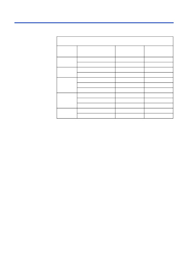
Table 13
shows the number of DQ pin groups per device.
Note to
Table 13
:
(1)
EP1C3 devices in the 100-pin TQFP package do not have any DQ pin groups in I/O
bank 1.
A programmable delay chain on each DQS pin allows for either a 90°
phase shift (for DDR SDRAM), or a 72° phase shift (for FCRAM) which
automatically center-aligns input DQS synchronization signals within the
data window of their corresponding DQ data signals. The phase-shifted
DQS signals drive the global clock network. This global DQS signal clocks
DQ signals on internal LE registers.
These DQS delay elements combine with the PLL’s clocking and phase
shift ability to provide a complete hardware solution for interfacing to
high-speed memory.
The clock phase shift allows the PLL to clock the DQ output enable and
output paths. The designer should use the following guidelines to meet
133 MHz performance for DDR SDRAM and FCRAM interfaces:
■
■
The DQS signal must be in the middle of the DQ group it clocks
Resynchronize the incoming data to the logic array clock using
successive LE registers or FIFO buffers
LE registers must be placed in the LAB adjacent to the DQ I/O pin
column it is fed by
■
Table 13. DQ Pin Groups
Device
Package
Number of
×
8 DQ
Pin Groups
Total DQ Pin
Count
EP1C3
100-pin TQFP
(1)
144-pin TQFP
324-pin FineLine BGA
400-pin FineLine BGA
144-pin TQFP
240-pin PQFP
256-pin FineLine BGA
240-pin PQFP
256-pin FineLine BGA
324-pin FineLine BGA
324-pin FineLine BGA
400-pin FineLine BGA
3
4
8
8
4
4
4
4
4
8
8
8
24
32
64
64
32
32
32
32
32
64
64
64
EP1C4
EP1C6
EP1C12
EP1C20
相關(guān)PDF資料 |
PDF描述 |
|---|---|
| EP1C6Q240I6 | NO POLISH CONNECTOR KIT |
| EP1C6Q240I7 | Cyclone FPGA Family |
| EP1C6Q240I8 | Cyclone FPGA Family |
| EP1C6Q256C6 | Cyclone FPGA Family |
| EP1C6Q256C7 | Cyclone FPGA Family |
相關(guān)代理商/技術(shù)參數(shù) |
參數(shù)描述 |
|---|---|
| EP1C6Q240C8N | 功能描述:FPGA - 現(xiàn)場(chǎng)可編程門陣列 FPGA - Cyclone I 598 LABs 185 IOs RoHS:否 制造商:Altera Corporation 系列:Cyclone V E 柵極數(shù)量: 邏輯塊數(shù)量:943 內(nèi)嵌式塊RAM - EBR:1956 kbit 輸入/輸出端數(shù)量:128 最大工作頻率:800 MHz 工作電源電壓:1.1 V 最大工作溫度:+ 70 C 安裝風(fēng)格:SMD/SMT 封裝 / 箱體:FBGA-256 |
| EP1C6Q240I7 | 功能描述:FPGA - 現(xiàn)場(chǎng)可編程門陣列 FPGA - Cyclone I 598 LABs 185 IOs RoHS:否 制造商:Altera Corporation 系列:Cyclone V E 柵極數(shù)量: 邏輯塊數(shù)量:943 內(nèi)嵌式塊RAM - EBR:1956 kbit 輸入/輸出端數(shù)量:128 最大工作頻率:800 MHz 工作電源電壓:1.1 V 最大工作溫度:+ 70 C 安裝風(fēng)格:SMD/SMT 封裝 / 箱體:FBGA-256 |
| EP1C6Q240I7N | 功能描述:FPGA - 現(xiàn)場(chǎng)可編程門陣列 FPGA - Cyclone I 598 LABs 185 IOs RoHS:否 制造商:Altera Corporation 系列:Cyclone V E 柵極數(shù)量: 邏輯塊數(shù)量:943 內(nèi)嵌式塊RAM - EBR:1956 kbit 輸入/輸出端數(shù)量:128 最大工作頻率:800 MHz 工作電源電壓:1.1 V 最大工作溫度:+ 70 C 安裝風(fēng)格:SMD/SMT 封裝 / 箱體:FBGA-256 |
| EP1C6T144C6 | 功能描述:FPGA - 現(xiàn)場(chǎng)可編程門陣列 FPGA - Cyclone I 598 LABs 98 IOs RoHS:否 制造商:Altera Corporation 系列:Cyclone V E 柵極數(shù)量: 邏輯塊數(shù)量:943 內(nèi)嵌式塊RAM - EBR:1956 kbit 輸入/輸出端數(shù)量:128 最大工作頻率:800 MHz 工作電源電壓:1.1 V 最大工作溫度:+ 70 C 安裝風(fēng)格:SMD/SMT 封裝 / 箱體:FBGA-256 |
| EP1C6T144C6N | 功能描述:FPGA - 現(xiàn)場(chǎng)可編程門陣列 FPGA - Cyclone I 598 LABs 98 IOs RoHS:否 制造商:Altera Corporation 系列:Cyclone V E 柵極數(shù)量: 邏輯塊數(shù)量:943 內(nèi)嵌式塊RAM - EBR:1956 kbit 輸入/輸出端數(shù)量:128 最大工作頻率:800 MHz 工作電源電壓:1.1 V 最大工作溫度:+ 70 C 安裝風(fēng)格:SMD/SMT 封裝 / 箱體:FBGA-256 |
發(fā)布緊急采購(gòu),3分鐘左右您將得到回復(fù)。