- 您現(xiàn)在的位置:買賣IC網(wǎng) > PDF目錄362655 > EL8203IY-T7 (INTERSIL CORP) 500MHz Rail-to-Rail Amplifiers PDF資料下載
參數(shù)資料
| 型號(hào): | EL8203IY-T7 |
| 廠商: | INTERSIL CORP |
| 元件分類: | 音頻/視頻放大 |
| 英文描述: | 500MHz Rail-to-Rail Amplifiers |
| 中文描述: | 1 CHANNEL, VIDEO AMPLIFIER, PDSO8 |
| 封裝: | MO-187, MSOP-8 |
| 文件頁(yè)數(shù): | 3/16頁(yè) |
| 文件大小: | 739K |
| 代理商: | EL8203IY-T7 |
第1頁(yè)第2頁(yè)當(dāng)前第3頁(yè)第4頁(yè)第5頁(yè)第6頁(yè)第7頁(yè)第8頁(yè)第9頁(yè)第10頁(yè)第11頁(yè)第12頁(yè)第13頁(yè)第14頁(yè)第15頁(yè)第16頁(yè)
3
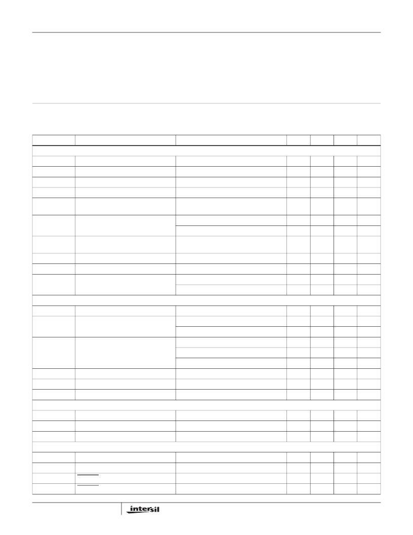
IMPORTANT NOTE: All parameters having Min/Max specifications are guaranteed. Typ values are for information purposes only. Unless otherwise noted, all tests are
at the specified temperature and are pulsed tests, therefore: T
J
= T
C
= T
A
Absolute Maximum Ratings
(T
A
= 25°C)
Supply Voltage from V
S
+ to V
S
- . . . . . . . . . . . . . . . . . . . . . . . . 5.5V
Input Voltage . . . . . . . . . . . . . . . . . . . . . . . . V
S
+ +0.3V to V
S
- -0.3V
Differential Input Voltage . . . . . . . . . . . . . . . . . . . . . . . . . . . . . . . .2V
Continuous Output Current . . . . . . . . . . . . . . . . . . . . . . . . . . . 40mA
Power Dissipation . . . . . . . . . . . . . . . . . . . . . . . . . . . . . See Curves
Storage Temperature. . . . . . . . . . . . . . . . . . . . . . . .-65°C to +150°C
Ambient Operating Temperature . . . . . . . . . . . . . . . .-40°C to +85°C
Operating Junction Temperature . . . . . . . . . . . . . . . . . . . . . .+125°C
CAUTION: Stresses above those listed in “Absolute Maximum Ratings” may cause permanent damage to the device. This is a stress only rating and operation of the
device at these or any other conditions above those indicated in the operational sections of this specification is not implied.
Electrical Specifications
V
S
+
= 5V, V
S
-
= GND, T
A
= 25°C, V
CM
= 2.5V, R
L
to 2.5V, A
V
= 1, Unless Otherwise Specified
PARAMETER
DESCRIPTION
CONDITIONS
MIN
TYP
MAX
UNIT
INPUT CHARACTERISTICS
V
OS
Offset Voltage
-8
-0.8
+8
mV
TCV
OS
Offset Voltage Temperature Coefficient
Measured from T
MIN
to T
MAX
3
μV/°C
IB
Input Bias Current
V
IN
= 0V
-9
-6
μA
I
OS
Input Offset Current
V
IN
= 0V
0.1
0.6
μA
TCI
OS
Input Bias Current Temperature
Coefficient
Measured from T
MIN
to T
MAX
2
nA/°C
CMRR
Common Mode Rejection Ratio
V
CM
= -0.15V to +3.5V (EL8202,EL8203)
70
95
dB
V
CM
= -0.15V to +3.5V (EL8403)
60
85
dB
CMIR
Common Mode Input Range
V
S
- -
0.15
V
S
+ -
1.5
V
R
IN
Input Resistance
Common Mode
3.5
M
C
IN
Input Capacitance
0.5
pF
AVOL
Open Loop Gain
V
OUT
= +1.5V to +3.5V, R
L
= 1k
to GND
V
OUT
= +1.5V to +3.5V, R
L
= 150
to GND
75
90
dB
80
dB
OUTPUT CHARACTERISTICS
R
OUT
Output Resistance
A
V
= +1
R
L
= 1k
R
L
= 150
R
L
= 150
R
L
= 1k
(EL8202,EL8203)
R
L
= 1k
(EL8403)
30
m
V
OP
Positive Output Voltage Swing
4.85
4.9
V
4.6
4.7
V
V
ON
Negative Output Voltage Swing
100
150
mV
25
50
mV
50
100
mV
I
OUT
Linear Output Current
65
mA
I
SC
(source)
Short Circuit Current
R
L
= 10
R
L
= 10
60
80
mA
I
SC
(sink)
Short Circuit Current
120
150
mA
POWER SUPPLY
PSRR
Power Supply Rejection Ratio
V
S
+ = 4.5V to 5.5V
70
95
dB
I
S-ON
Supply Current - Enabled (per amplifier)
5.6
6.2
mA
I
S-OFF
Supply Current - Disabled (per amplifier)
40
90
μA
ENABLE (EL8202 ONLY)
t
EN
Enable Time
200
ns
t
DS
Disable Time
25
ns
V
IH-ENB
ENABLE Pin Voltage for Power-up
0.8
V
V
IL-ENB
ENABLE Pin Voltage for Shut-down
2
V
EL8202, EL8203, EL8403
相關(guān)PDF資料 |
PDF描述 |
|---|---|
| EL8203IS-T13 | 500MHz Rail-to-Rail Amplifiers |
| EL8203IS-T7 | 500MHz Rail-to-Rail Amplifiers |
| EL8403IUZ-T7 | 500MHz Rail-to-Rail Amplifiers |
| EL8203IY-T13 | 500MHz Rail-to-Rail Amplifiers |
| EL8202IYZ-T13 | 500MHz Rail-to-Rail Amplifiers |
相關(guān)代理商/技術(shù)參數(shù) |
參數(shù)描述 |
|---|---|
| EL825 | 制造商:Everlight Electronics Co 功能描述:OPTOCOUPLER DARLINGTON O/P DIP-4 制造商:Everlight Electronics Co 功能描述:OPTOCOUPLER, DARLINGTON, O/P, DIP-4 |
| EL825(M)(TA)-V | 制造商:EVERLIGHT 制造商全稱:Everlight Electronics Co., Ltd 功能描述:4 PIN DIP PHOTOTRANSISTOR |
| EL825(M)(TB)-V | 制造商:EVERLIGHT 制造商全稱:Everlight Electronics Co., Ltd 功能描述:4 PIN DIP PHOTOTRANSISTOR |
| EL825(S)(TA)-V | 制造商:EVERLIGHT 制造商全稱:Everlight Electronics Co., Ltd 功能描述:4 PIN DIP PHOTOTRANSISTOR |
| EL825(S)(TB)-V | 制造商:EVERLIGHT 制造商全稱:Everlight Electronics Co., Ltd 功能描述:4 PIN DIP PHOTOTRANSISTOR |
發(fā)布緊急采購(gòu),3分鐘左右您將得到回復(fù)。