- 您現(xiàn)在的位置:買賣IC網(wǎng) > PDF目錄97880 > EDI7P005FLC0202I15 xDSL Differential Line Driver; Temperature Range: -40°C to 85°C; Package: 16-QFN T&R PDF資料下載
參數(shù)資料
| 型號(hào): | EDI7P005FLC0202I15 |
| 英文描述: | xDSL Differential Line Driver; Temperature Range: -40°C to 85°C; Package: 16-QFN T&R |
| 中文描述: | 周邊雜項(xiàng) |
| 文件頁(yè)數(shù): | 6/12頁(yè) |
| 文件大小: | 121K |
| 代理商: | EDI7P005FLC0202I15 |
August 2000 Rev. 3 - ECO #13127
3
PCMCIA Flash Memory Card
FLC Series
PC Card Products
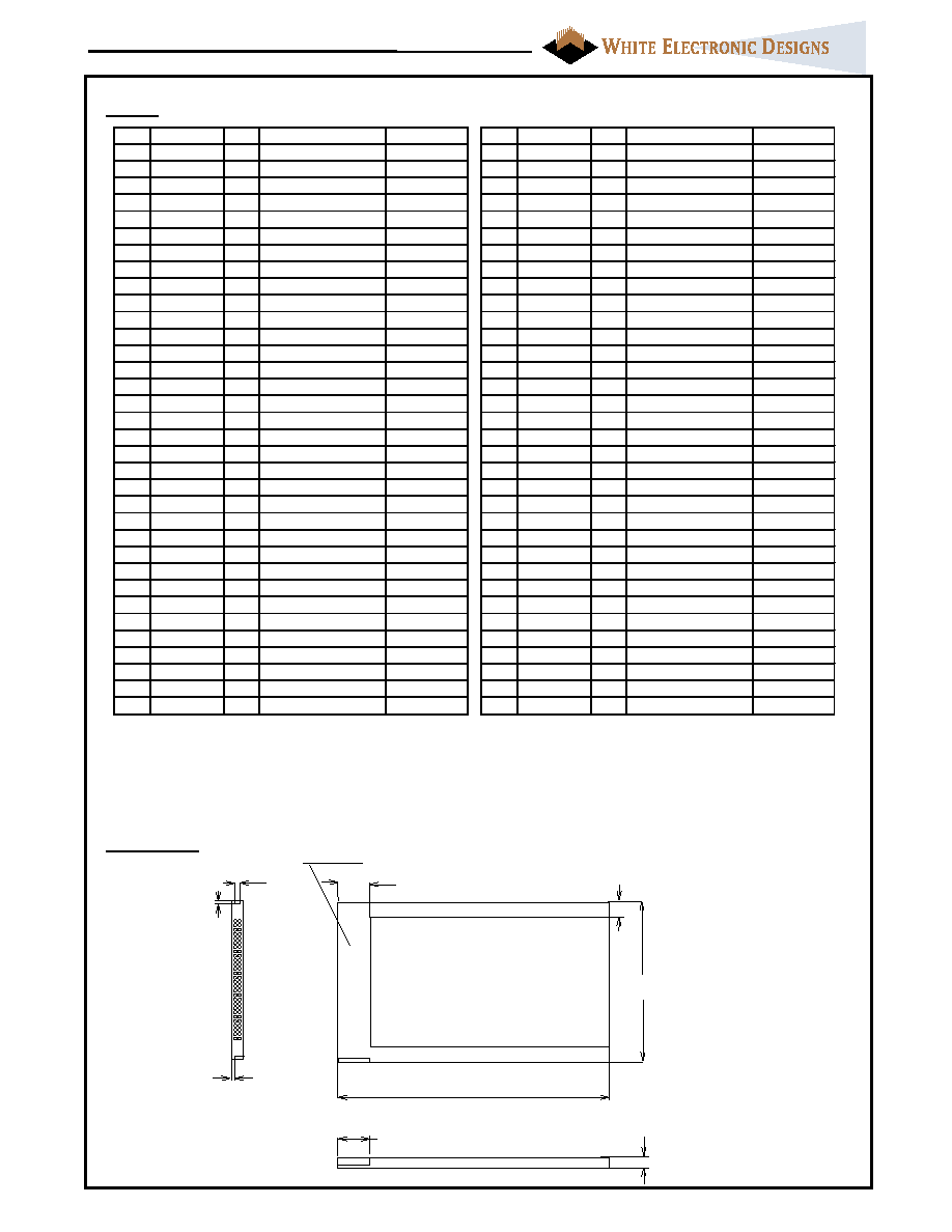
Pinout
Notes:
1. Wait#, BVD1 and BVD2 are driven high for compatibility
2. Shows density for which specified address bit is MSB. Higher order address bits are N.C.
(i.e. 4MB A21 is MSB A22 - A25 are NC).
3. For the 3MB card the memory will wrap at the 4MB boundary, for 5MB, 6MB, and & 7MB cards the memory
will wrap at the 8MB boundary, for 9MB and 10MB cards the memory will wrap at the 16MB boundary.
Mechanical
54.0mm
± 0.10
(2.126”)
10.0mm MIN
(0.400”)
1.6mm
± 0.05
(0.063”)
1.0mm
± 0.05
(0.039”)
1.0mm
± 0.05
(0.039”)
3.3mm
± T1 (0.130”)
T1=0.10mm interconnect area
T1=0.20mm substrate area
Interconnect area
10.0mm MIN
(0.400”)
3.0mm MIN
85.6mm
± 0.20
(3.370”)
Substrate area
Pin Signal name I/O
Function
Active
Pin Signal name I/O
Function
Active
1
GND
Ground
35
GND
Ground
2
DQ3
I/O
Data bit 3
36
CD1#
O
Card Detect 1
LOW
3
DQ4
I/O
Data bit 4
37
DQ11
I/O
Data bit 11
4
DQ5
I/O
Data bit 5
38
DQ12
I/O
Data bit 12
5
DQ6
I/O
Data bit 6
39
DQ13
I/O
Data bit 13
6
DQ7
I/O
Data bit 7
40
DQ14
I/O
Data bit 14
7
CE1#
I
Card enable 1
LOW
41
DQ15
I
Data bit 15
8
A10
I
Address bit 10
42
CE2#
I
Card Enable 2
LOW
9
OE#
I
Output enable
LOW
43
VS1
O
Voltage Sense 1
N.C.
10
A11
I
Address bit 11
44
RFU
Reserved
N.C.
11
A9
I
Address bit 9
45
RFU
Reserved
N.C.
12
A8
I
Address bit 8
46
A17
I
Address bit 17
13
A13
I
Address bit 13
47
A18
I
Address bit 18
14
A14
I
Address bit 14
48
A19
I
Address bit 19
1MB(2)
15
WE#
I
Write Enable
LOW
49
A20
I
Address bit 20
16
RDY/BSY#
O
Ready/Busy
N.C.
50
A21
I
Address bit 21
4MB(2,3)
17
Vcc
Supply Voltage
51
Vcc
Supply Voltage
18
Vpp1
Prog. Voltage
N.C.
52
Vpp2
Prog. Voltage
N.C.
19
A16
I
Address bit 16
53
A22
I
Address bit 22
8MB(2,3)
20
A15
I
Address bit 15
54
A23
I
Address bit 23
16/10MB(2,3)
21
A12
I
Address bit 12
55
A24
I
Address bit 24
N.C.
22
A7
I
Address bit 7
56
A25
I
Address bit 25
N.C.
23
A6
I
Address bit 6
57
VS2
O
Voltage Sense 2
N.C.
24
A5
I
Address bit 5
58
RST
I
Card Reset
N.C.
25
A4
I
Address bit 4
59
Wait#
O
Extended Bus cycle
LOW(1)
26
A3
I
Address bit 3
60
RFU
Reserved
N.C.
27
A2
I
Address bit 2
61
REG#
I
Attrib Mem Select
LOW
28
A1
I
Address bit 1
62
BVD2
O
Bat. Volt. Detect 2
(1)
29
A0
I
Address bit 0
63
BVD1
O
Bat. Volt. Detect 1
(1)
30
DQ0
I/O
Data bit 0
64
DQ8
I/O
Data bit 8
31
DQ1
I/O
Data bit 1
65
DQ9
I/O
Data bit 9
32
DQ2
I/O
Data bit 2
66
DQ10
O
Data bit 10
33
WP
O
Write Potect
HIGH
67
CD2#
O
Card Detect 2
LOW
34
GND
Ground
68
GND
Ground
相關(guān)PDF資料 |
PDF描述 |
|---|---|
| EDI7P005FLC0300C15 | xDSL Differential Line Driver; Temperature Range: -40°C to 85°C; Package: 16-QFN T&R |
| EDI7P005FLC0300I15 | xDSL Differential Line Driver; Temperature Range: -40°C to 85°C; Package: 8-SOIC |
| EDI7P005FLC0301C15 | xDSL Differential Line Driver; Temperature Range: -40°C to 85°C; Package: 8-SOIC T&R |
| EDI7P005FLC0301I15 | xDSL Differential Line Driver; Temperature Range: -40°C to 85°C; Package: 8-SOIC T&R |
| EDI7P005FLC0302C15 | xDSL Differential Line Driver; Temperature Range: -40°C to 85°C; Package: 10-HMSOP |
相關(guān)代理商/技術(shù)參數(shù) |
參數(shù)描述 |
|---|---|
| EDI7P005FLC0300C15 | 制造商:未知廠家 制造商全稱:未知廠家 功能描述:Peripheral Miscellaneous |
| EDI7P005FLC0300I15 | 制造商:未知廠家 制造商全稱:未知廠家 功能描述:Peripheral Miscellaneous |
| EDI7P005FLC0301C15 | 制造商:未知廠家 制造商全稱:未知廠家 功能描述:Peripheral Miscellaneous |
| EDI7P005FLC0301I15 | 制造商:未知廠家 制造商全稱:未知廠家 功能描述:Peripheral Miscellaneous |
| EDI7P005FLC0302C15 | 制造商:未知廠家 制造商全稱:未知廠家 功能描述:Peripheral Miscellaneous |
發(fā)布緊急采購(gòu),3分鐘左右您將得到回復(fù)。