- 您現(xiàn)在的位置:買賣IC網(wǎng) > PDF目錄93290 > EC4301C PDF資料下載
參數(shù)資料
| 型號: | EC4301C |
| 文件頁數(shù): | 2/4頁 |
| 文件大小: | 29K |
| 代理商: | EC4301C |
EC4301C
No.7014-2/4
Continued from preceding page.
Ratings
Parameter
Symbol
Conditions
min
typ
max
Unit
Input Capacitance
Ciss
VDS=--10V, f=1MHz
7.5
pF
Output Capacitance
Coss
VDS=--10V, f=1MHz
5.7
pF
Reverse Transfer Capacitance
Crss
VDS=--10V, f=1MHz
1.8
pF
Turn-ON Delay Time
td(on)
See specified Test Circuit.
24
ns
Rise Time
tr
See specified Test Circuit.
55
ns
Turn-OFF Delay Time
td(off)
See specified Test Circuit.
120
ns
Fall Time
tf
See specified Test Circuit.
130
ns
Total Gate Charge
Qg
VDS=--10V, VGS=--10V, ID=--100mA
1.43
nC
Gate-to-Source Charge
Qgs
VDS=--10V, VGS=--10V, ID=--100mA
0.18
nC
Gate-to-Drain “Miller” Charge
Qgd
VDS=--10V, VGS=--10V, ID=--100mA
0.25
nC
Diode Forward Voltage
VSD
IS=--100mA, VGS=0
--0.91
--1.2
V
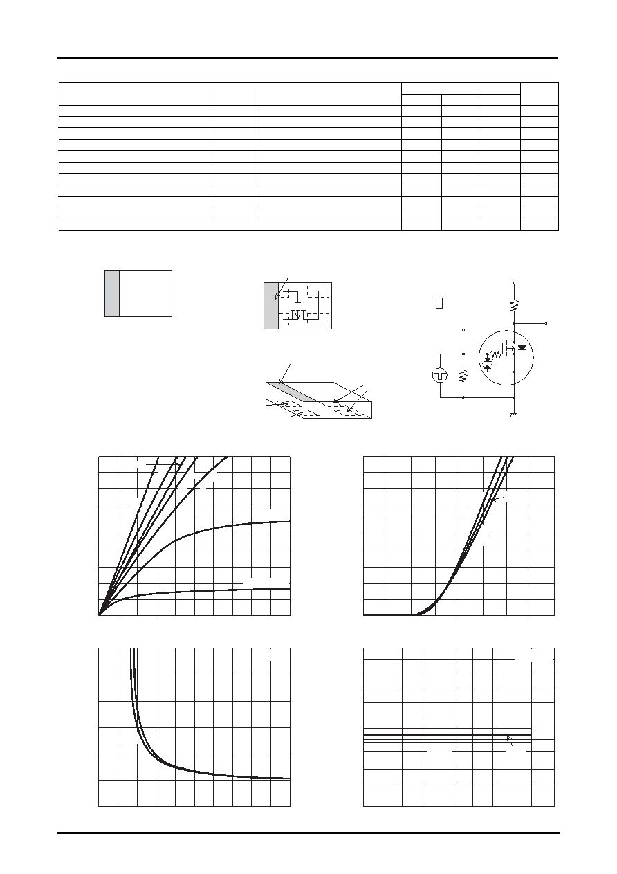
Type No. Indication(Top view)
Electrical Connection(Top view)
Switching Time Test Circuit
PW=10
s
D.C.
≤1%
0V
--4V
VIN
P.G
50
G
S
ID= --50mA
RL=300
VDD= --15V
VOUT
VIN
D
EC4301C
0
--0.01
--0.02
--0.03
--0.04
--0.06
--0.07
--0.08
--0.09
--0.10
--0.4
--0.05
--0.8
--1.2
--1.6
--2.0
--0.2
--0.6
--1.0
--1.4
--1.8
ID -- VDS
VGS= --1.5V
--3.5V
--6.0V
--2.0V
--4.0V
--3.0V --2.5V
0
--0.5
--1.0
--1.5
--2.0
--2.5
--3.0
--4.0
--3.5
0
--0.02
--0.04
--0.06
--0.08
--0.10
--0.12
--0.14
--0.16
--0.18
--0.20
ID -- VGS
VDS= --10V
IT00077
IT00078
T
a=
--25
°C
25
°C
75
°C
Drain-to-Source Voltage, VDS -- V
Drain
Current,
I
D
-
A
Gate-to-Source Voltage, VGS -- V
Drain
Current,
I
D
-
A
0
--1
--2
--3
5
--4
10
--5
15
20
25
--6
30
--7
--8
--9
--10
RDS(on) -- VGS
Ta=25
°C
--0.01
1.0
--0.1
23
5
7
23
100
7
5
3
2
10
7
5
3
2
RDS(on) -- ID
VGS= --4V
IT00079
IT00080
Ta=75
°C
25
°C
--25
°C
ID= --30mA --50mA
Static
Drain-to-Source
On-State
Resistance,
R
DS
(on)
-
Static
Drain-to-Source
On-State
Resistance,
R
DS
(on)
-
Gate-to-Source Voltage, VGS -- V
Drain Current, ID -- A
Gate
Source
Gate
Drain
Polarity mark (Top)
*Electrodes : on the bottom
Polarity mark (Top)
R
相關(guān)PDF資料 |
PDF描述 |
|---|---|
| EC4302C | |
| EC4303C | TRANSISTOR | MOSFET | P-CHANNEL | 50V V(BR)DSS | 70MA I(D) | LLCC |
| EC4402C | |
| EC4403C | |
| EC4A01C | |
相關(guān)代理商/技術(shù)參數(shù) |
參數(shù)描述 |
|---|---|
| EC4301C_06 | 制造商:SANYO 制造商全稱:Sanyo Semicon Device 功能描述:Small Signal Switch and Interface Applications |
| EC4302C | 制造商:未知廠家 制造商全稱:未知廠家 功能描述: |
| EC4302C_06 | 制造商:SANYO 制造商全稱:Sanyo Semicon Device 功能描述:Small Signal Switch and Interface Applications |
| EC4303C | 制造商:未知廠家 制造商全稱:未知廠家 功能描述:TRANSISTOR | MOSFET | P-CHANNEL | 50V V(BR)DSS | 70MA I(D) | LLCC |
| EC4305C | 制造商:SANYO 制造商全稱:Sanyo Semicon Device 功能描述:P-Channel Silicon MOSFET General-Purpose Switching Device Applications |
發(fā)布緊急采購,3分鐘左右您將得到回復(fù)。